Introduction of Single Chip Packaging (SCP) - Fitech Solder Paste

Introduction of Single Chip Packaging (SCP) - Fitech Solder Paste
SCP is a relatively simple and widely used packaging method, which has accumulated a massive application experience. SCP forms a microelectronic device by packaging a single chip. Packaging materials are often made of low-cost plastics and ceramics with high thermal performance and reliability. SCP process starts with dicing wafers, followed by packaging chips and testing samples. The package can be put into production after the results are qualified.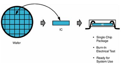
Figure 1. The basic process of single chip packaging.
The electrical signal connection of the chip needs to be realized through bonding. The chip needs to be fixed to a specific substrate in some ways, such as wire bonding, flip-chip bonding, solder connection, or conductive adhesive connection. Wire bonding is the most widely used bonding method at present, which requires to connects the chip electrodes and the substrate pads by using gold wires, aluminum wires, or other metals with excellent ductility and conductivity. Flip-chip bonding enables more I/Os. For flip-chip bonding, solder paste will be deposited around the chips, or micro bumps will be formed by planting balls on the chip pads. The surface of the chip is turned down and fitted with the preformed pads on the substrates. The interconnection substrate can be PCB, ceramic material, chip carrier, or ball grid array package.
In order to further improve the performance of electronic devices, the level of integrated circuits is progressing faster and faster, which requires a large number of I/Os in packaging. In order to meet these requirements, more leads and smaller pitches are required in the package cavity.
Dual Inline Package (DIP)
DIP is a common single-chip microcomputer structure, and leads are soldered on both sides of the DIP. These leads can be inserted into the plated holes in the PCB to achieve electrical pathways. DIP has a small number of leads(8-64). More leads are less common. The chip is bonded to the lead frame through metal wires, and the lead frame is extended to form the leads. Manufacturers often package chips in plastic, epoxy, or ceramic. After coating the solder paste on the plated holes, the leads can be inserted and soldered to form solder joints
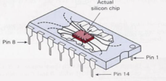
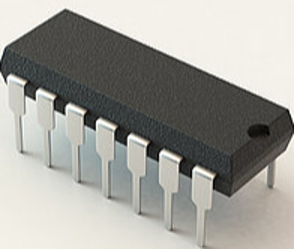
Figure 2. DIP structure.
Quad Flat Pack (QFP)
QFP can be metal or ceramic cavity packages or plastic molded packages. The leads extend from all four sides. The QFP can have more than 300 leads at most, which is far more than that of the DIP. QFP can allow a single chip or multiple chips to be packaged and can be used in more highly integrated devices. The leads of QFP will be bent into a gull-wing shape and mounted on the pad position of the substrate, which is very different from the through-hole technology. The bonding materials for device mounting usually adopt solder paste, which solidifies into solder joints after reflow.

Figure 3. QFP appearance.
Ball Grid Array (BGA)
The purpose of BGA is to solder the device on the PCB after completing the first-level packaging of the chip. The emergence of BGA technology is due to the fact that the number of I/Os of other old-fashioned packages (such as QFP) has reached the bottleneck. More advanced packaging technology is required to achieve more I/Os. The packaging form of BGA is similar to flip-chip bonding, and solder joints are generated by ball planting and reflow soldering. BGA is a very flexible packaging form. The chip can be wire bonded and connected to the substrate pad, or it can be ball-planted and flip-chip bonded to the pad and then packaged. After packaging, balls are planted on the exposed pad at the bottom of the single-chip device and soldered on the PCB. Although the BGA package has a large number of bumps and a larger I/O pitch, the overall size is still small.
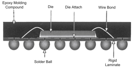
Figure 4. BGA schematic diagram.
Pin Grid Array (PGA)
PGA is also a very traditional packaging technology. PGA components are rectangular or square in shape with rows of leads or a full array of leads at the bottom. Similar to DIPs, the leads of PGAs are mainly inserted into plated holds. PGAs are better suited for processors with wider data bus widths than DIPs because PGAs can provide a higher lead count and handle a specific number of connection points better. In terms of price, PGA is cheaper than BGA or other grid arrays, but the thermoelectric performance of PGA is not enough to meet higher demands, and its application range is smaller than BGA.
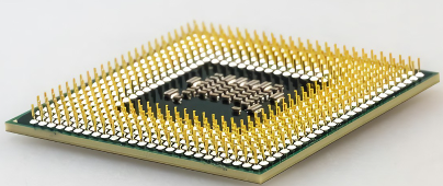
Figure 5. PGA appearance.
Shenzhen Fitech can provide customers with ultra-fine solder paste products, including SAC305 solder paste, Sn42Bi57.6Ag0.4 solder paste, etc., which can be used for through-hole insertion, SMT, and reflow soldering processes of components. What’s more, the products can also be used for printing and manufacturing solder paste dots, which can replace the ball-planting process.




 Back to list


