Ultra-Fine-Pitch Soldering of Mini/Micro LED - Solder Paste, Epoxy Solder Paste, Die Bond Solder Paste and Flux for Micro LED
In 1993, the high-brightness blue LED based on GaN was born. All three primary color LEDs of red, green, and blue used to realize full-color display have been discovered. The LED display has entered the era of full-color light. LED display has developed rapidly in terms of raw materials, technologies, display effects, and applications. The pixels of LED displays are shrinking at a rate of about 1mm per year. After nearly 30 years of rapid development, LED displays have replaced LCD and DLP applications in indoor command and monitoring centers, cultural media, radio and television studios, cinema screens, and smart cities.

With the continuous development of LED display technology, the market's requirements for better picture quality and visual experience make the miniaturization of pixel units an inevitable trend in high-end applications. The ultra-high-density microLED display has many features better than traditional display technologies, such as high brightness, high definition, high color saturation, seamless infinite splicing, etc. Due to the extraordinary advantages, the companies in the industry highly value the technology of microLED.
 \
\
Mini/Micro LED display refers to the display screen with an LED pixel pitch smaller than 1.0mm. The pixel pitch of 80-175 inch 4K and 8K ultra-high-definition large-size LED display products is generally between 0.4mm and 0.8mm. Light-emitting chip with a small size has been regarded as a fine display category, and dot pitch has been classified into a sub-millimeter display category. Infrared touch, human-computer interaction, and applications, microLED have entered the fields of super TV, high-end business, remote video conference, high-end medical treatment, education, and exhibition.
There are three main packaging routes for microLED display, including SMD, IMD, and COB. Flip-chip COB is regarded as the development direction of micro-LED packaging due to the advantages of higher pixel density, smaller dot pitch, higher reliability, low cost, and huge development potential of ultra-large size and ultra-high pixel density.
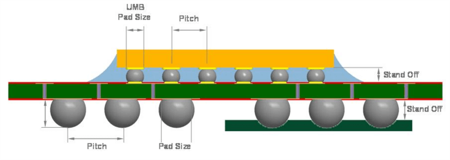
However, flip-chip COB packaging has several technical problems. The flip-chip LED integrated packaging technology is mainly optimized and improved in terms of chip transfer, bonding, packaging, and optical design. In terms of chip soldering, small micro-pitch display chips and small pixel pitch are the factors that influence the selectivity of solder paste. Under the microLED display design, the size of the flip-chip is less than 200um, and the distance between the chip electrodes is less than 100um. Taking a 4milx 8mil (100um x 200um) chip as an example, its pad size is about 34um × 70um. According to the eight-ball principle, the diameter of a solder ball should not exceed 4.25um. As a result, T9 solder pastes cannot meet the soldering requirements because of reduced soldering reliability. However, Fitech’s T10 solder paste and epoxy solder paste for fine-pitch soldering can still fulfill the soldering requirements. The products meet the soldering requirements of LED display chips with a minimum pad size of 24um × 24um. In addition, the ball-attach process is appropriate for small-sized microLED display chips. The highly reliable no-clean flux, water-soluble flux, and epoxy flux produced by Fitech are effective for the mico LED chip soldering of pre-evaporated solder joints.
Soldering accuracy is another problem that has to consider. Chip transfer is achieved by a high-speed die-bonding machine using the multi-swing arm needle transfer method. In the processes of chip transfer, die bond, and bonding, the deviation of die bonding accuracy and angle accuracy are likely to occur. When transferring the LED chip from the epitaxial wafer to the blue film, the angle will be deflected. The blue film will be pulled during the die-bonding process, which may intensify the deflection. During the reflow soldering process, the melting of solder may cause a slight offset of flip chips. These deviations will affect the accuracy, and thus affect the product reliability. Due to the small chip size and pixel pitch of the microLED display chip, the ±25um of die-bonding accuracy deviation and the ±2° of off-angle deviation in the X-axis and Y-axis will be significantly magnified. Fitech’s epoxy solder paste and epoxy flux have self-assembly and self-correction functions to prevent offset during reflow soldering. Both products more or less self-correct the deviation generated in the previous process, which can effectively enhance soldering accuracy. Fitech’s products are suitable for the high-precision and high-reliability packaging of microelectronic devices and other fields. The products are applicable to wafer bump soldering, chip soldering using evaporation solder, BGA, SIP, CSP, microLED packaging, integrated circuit packaging, etc.
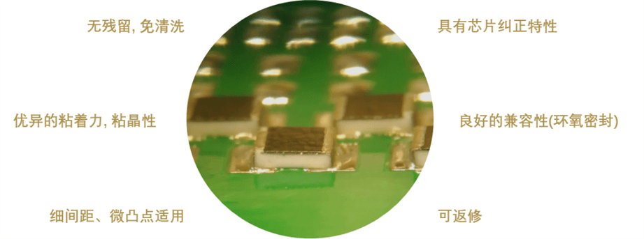
The third problem is solder paste stability. The chip size and pixel pitch are getting smaller, increasing the pixel density. Due to the high pixel density of microLED displays, a massive number of LED chips should be transferred. As a result, the operating time from solder paste addition to the die transfer to reflow soldering becomes longer. Therefore, it is essential to choose solder paste with outstanding stability for various properties. Because of the advanced preparation technology of ultra-fine alloy solder powder, Fitech produces alloy solder powder with a narrow particle size distribution, excellent sphericity, low oxygen content, and high purity. The solder powder is combined with self-developed high-reliability flux to produce die-bonding solder paste for micro-LED display chips. The alloy solder powder particles are perfectly spherical, and the surface is smooth and flat. Thus, the stability of rheological properties and performance of the solder paste products can be ensured, and the service life of the dispensers and jet printing machines can be improved.
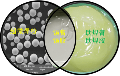
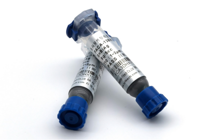
Fitech’s ultra-fine-pitch soldering products for microLED.

Fitech has accumulated many years of experience in the microelectronic soldering industry and has developed many adaptive products for the market or individual customers. Fitech is a world-leading material and solution provider of microelectronics and semiconductor packaging. In addition, Fitech is a national high-tech enterprise engaged in the microelectronics and semiconductor packaging material industry.Fitech has complete production lines of solder powder and related products. Fitech is the manufacturer of electronic-grade packaging materials that can produce T2-T10 ultra-fine alloy solder powder. Solder paste, epoxy solder paste, and alloy solder powder developed by Fitech are widely used in various microelectronics and semiconductor packaging. The global SMT electronic chemical manufacturers, micro-photoelectric manufacturers, and semiconductor packaging testers have acknowledged the products. However, the problems with microelectronics and semiconductor packaging materials are extensive. Here we only describe the common issues. Due to different technological processes, the problems involved may also be different. Fitech sincerely welcomes you to discuss specific issues with our professionals. We hope to keep pace with the times with our partners and explore new problems, new technologies, and complex processes together. We strive to provide our partners with professional packaging and soldering material services for microelectronics and semiconductors.
-End-






 Back to list


