Types of Void Defects in Microelectronic Packaging Solder Joints
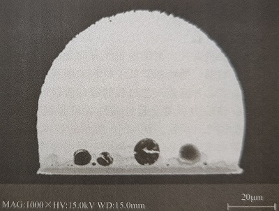
With wide application of lead-free solder pastes, it is found that various reliability problems will occur when applying lead-free solder pastes. One of the issues affecting solder joint reliability is voids. There are six kinds of voids inside the solder joints formed by solders for microelectronic packaging, including macroscopic voids, micro via voids, planar microvoids, pin voids, shrink voids, and Kirkendall voids. The formation of voids has a non-negligible impact on the reliability of solder joints. The location, conditions, mechanism, and causes of the voids are different. In general, the formation of voids can affect heat conduction and cause a rapid decrease in the mechanical reliability of the solder joints. With the continuous development of electronic information technology, the size of solder joints is getting smaller and smaller, and the ratio of voids to the solder joint area is increasing. Therefore, the impact of voids on solder joints should be a concern.
Macroscopic voids: The diameter is 100 μm to 300 μm. The formation of macroscopic voids is due to the gas generated by the evaporation of the solder solvent and rheological additives fail to escape during reflow soldering. For example, in flip-chip, voids are produced at the UBM-solder interface after reflow soldering.

Micro via voids: High-Density Interconnects (HDI) use micro vias to satisfy the outer and inner layers of the PCBs. However, pads with vias often have voids formed in the solder joints due to the inability of the gas in the vias to escape. Micro via voids has a diameter of 100 μm or even larger, which affects the reliability of the inner layer system where the micro-via is located.
Planar microvoids: Microvoids with a diameter of 25 μm to 50 μm are distributed on the plane above the IMCs at the interface between the solder joints and the pads. It mostly occurs on the pads with an ImAg surface finish.
Pin voids: Poor copper plating on the PCB can cause pin-shaped holes in the copper layer, which can still be observed after OSP or ImAg surface treatment. These pin-holes can cause pin-shaped holes in or above the IMC layer.
Shrink voids: Strictly speaking, a shrink void is not necessarily a void but linear cracks with dendritic rough edges formed on the surface of the solder joints. These cracks are found on the surface of the SAC solder ball and are caused by the sequential solidification of the SAC solder, which is also known as thermal cracks.
Kirkendall voids: The diameter is 1 to 2 μm. Different metals have different diffusion rates during solid-state aging. The mutual diffusion is unbalanced, resulting in Kirkendall voids on the side of the metal with a faster diffusion rate.
The formation of voids is related to a variety of factors and is the result of comprehensive factors. However, as solder paste plays an important role in packaging and soldering, the problem of voids should be considered at the product design stage. When designing the solder paste formulation, the components leading to void formation should be concerned. Fitech specializes in the development and production of high-quality regular solder paste, epoxy solder paste, and solder powder. Fitech has rich experience in reducing the void ratio of solder joints. Welcome to inquire and cooperate with us.
-End-
*Disclaimer: Except for "reprinted" articles, the copyright of the original content published on this site belongs to Shenzhen Fitech. Without consent and authorization, it may not be reproduced, reproduced, quoted, changed, or published. This article is originally created by the author, and the content of the article is the author's personal opinion. "Reprint" is only to convey a different point of view and does not mean approval or support for the point of view. If there is any infringement, please contact us, and we will delete it!


 Back to list


