Device failure due to SMT wick effect-Shenzhen Fitech

Device failure due to SMT wick effect-Shenzhen Fitech
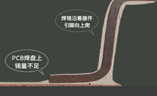
The wick effect, also known as the creeping tin effect, is an inherent characteristic of solder in the PCB soldering mechanism: "solder always flows from low temperature to high temperature", which means that the nature of solder is to go where the temperature is high. If the temperature of the device pins is high during soldering, the liquid solder will climb up the pins.

Figure 1. The wick effect and its effects
Basic conditions for the wick effect to occur
1. the pin can be wetted with solder and has good solderability, e.g. gold-plated pin terminals;
2. the pin temperature is higher than the pad temperature
3. sufficient heat so that the solder does not cure easily during the climbing process;
4. better solderability on the pins than on the PCB pads.
Wick effect failure mode
In principle, the wick effect does not cause failures when the PCB pad has sufficient tin. The wick effect causes the following failure modes:
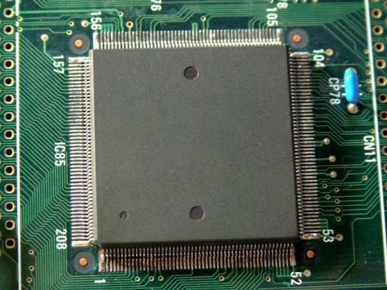
1. excessive amount of tin on the QFP pins, although the solder joints are normal, the solder creep causes the upper bend area of the gull wing foot to lose elasticity, reducing the ability of the pins to absorb mechanical and thermal stresses;

Figure 2. QFP package
2. the connector wick effect, solder through the plastic body of the device into the plug assembly area, affecting the performance of the assembly plug, judged as not acceptable;
3. wick effect causing a short circuit or open circuit in the solder joint;
4. the wick effect, where solder enters the device and causes functional failure.
How to prevent the wick effect?
1. use a segmentation scheme for device terminal handling to prevent excessive solder creep;
2. the device is moulded with the terminal and body in one piece to ensure close contact between the plastic body and the terminal;
3. reflow temperature profile control: to avoid excessive drop in PCB temperature and device body, such as PCB using carrier-assisted overReflow, the temperature of the lower temperature zone of the furnace is higher than the corresponding upper temperature zone temperature setting to effectively compensate for the large heat capacity impact of the board and carrier;
4. when the PCB pad solderability is poor and the device terminal solderability is good, Reflow constant temperature zone needs to have a certain length of time, so that the solder flux has sufficient time to remove the PCB pad oxide layer, to avoid the flux failure to remove the PCB pad surface oxide layer when the solder melts and the wick effect occurs.


 Back to list


