PCB Surface Treatment Composite Process - Immersion Gold + OSP

PCB Surface Treatment Composite Process - Immersion Gold + OSP
The PCB surface treatment composite process - Immersion Gold + OSP is a process combination commonly used in the manufacture of high-end electronics. This combination process combines a sinker plate with an OSP (Organic Solderability Preservatives) process to achieve a better overall result.
The intermetallic compound (IMC) in the solder joint of the sinker plate grows on the nickel layer, while the mechanical strength of the nickel-tin intergranules is slightly weaker than that of the copper-tin intergranules. The problem of insoluble black discs with high phosphorus content processes can arise in the immersed gold process, which is a difficult problem to solve. However, the sunken gold process still offers many advantages, such as a flat pad surface, the oxidation resistance and low resistivity properties of gold, and a wide process window.
Application of composite processes
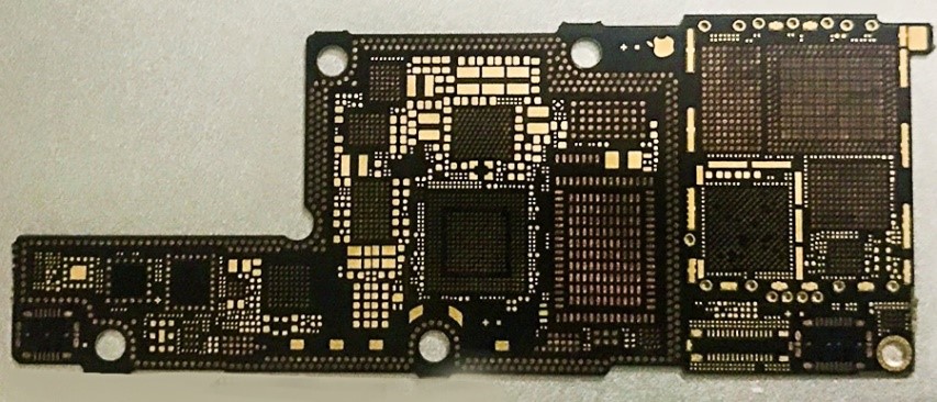
In order to combine mechanical strength with other advantages, the smartphone manufacturing industry commonly uses a composite process, i.e. a sink gold board + BGA area pads using the OSP process. This process allows the BGA solder joints to be grown directly onto the copper foil to ensure their mechanical strength. The composite process is a relatively complex manufacturing process, initially used in high-end smartphones, and is gradually becoming recognised and popular in the manufacturing of high-end electronics.

Figure 1. PCB surface treatment composite process: Apple mobile phone motherboard; where the BGA pads are OSP process and other areas of the pads surface treatment ENIG
Giovanni effect and insoluble gold surfaces in the sinker process
After the use of the gold sinking process, the pores on the gold surface may expose the nickel layer, which can lead to the Galvanic Effect in a corrosive environment, resulting in the dissolution of nickel (gold as cathode and nickel as anode). The dissolution of nickel can lead to the simultaneous reduction and deposition of copper ions in solution on the gold surface, resulting in a darkening of the gold skin film or even the appearance of metallic copper. Once copper is present on the surface after sinking the gold, the oxidised copper will cause the pads to refuse to solder and thus the problem of the gold surface not dissolving. This is a detail that needs attention.
In summary, electroless nickel-gold pads have a flat surface, are suitable for close pitch process requirements, can be baked and cleaned, and have a wide process window. The gold surface can be used as a contact surface or Wire bond substrate and the non-oxidising properties of gold give the immersed gold board good solderability.
Common disadvantages of the immersion gold process
However, there are also some common defects in electroless nickel-gold boards, including black pans due to abnormal control of the sink process (solder drops, insufficient strength of solder joints), inclusions of organic matter in the gold layer due to the sink process (refusal to solder, poor solder shrinkage), thin gold layers due to abnormal control of the high phosphorus content process (refusal to solder, solder shrinkage, pads not gold), residual plating solution due to abnormal PCB processes (refusal to solder, solder shrinkage, foreign matter (contamination), poor control of the sinking process leading to oxidation and contamination of the nickel layer (gold peeling, solder rejection, shrinkage), abnormal control of the sinking process leading to cracking of the nickel layer and separation from the copper layer (abnormal solder joint reliability). These issues require attention and control in the process.


 Back to list


