Lead-Free Solder Paste for MEMS Devices: Low Stress Packaging of MEMS Devices
Lead-Free Solder Paste for MEMS Devices: Low Stress Packaging of MEMS Devices
Solder Paste and Ultra-Fine Solder Manufacturer-Shenzhen Fitech is a comprehensive solder paste supplier integrating production, sales, research, and service of solder paste, epoxy solder paste, and solder powder. Fitech is the leading unit for the formulation of solder powder standards of the Ministry of Industry and Information Technology. Fitech's products include ultra-fine lead-free printing solder paste, ultra-fine lead-free dispensing solder paste, ultra-fine lead-free jetting solder paste, ultra-fine lead-free pin transfer solder paste, no-clean solder paste, water-soluble solder paste, high-temperature solder paste, medium-temperature solder paste, low-temperature solder paste, etc. Fitech can manufacture electronic-grade packaging solder powders with particle sizes from T2-T10.

Abstract: Packaging is one of the most important links in developing microelectromechanical systems (MEMS). Packaging determines the reliability and cost of MEMS devices and is the key to the practicality and commercialization of MEMS devices. However, the residual stress introduced in the packaging process will cause the offset of the output signal of the MEMS devices. Hence, the packaging stress gradually changes with time and seriously affects the reliability and long-term stability of the MEMS devices. Therefore, reducing packaging stress is a key factor in achieving high performance and stability. This article briefly analyzes the mechanism of MEMS device packaging stress in the process of chip-level packaging, introduces the current domestic and international stress reduction packaging technology and methods in detail, and makes a summary and prospect of MEMS device low-stress packaging technology.
Keywords: MEMS; sensor; low stress packaging; reliability; long-term stability
0 Preface
MEMS are micro-devices or micro-systems that integrate electricity and mechanics. MEMS follows the micro/nano micro-fabrication process of integrated circuit (IC) and is a complete and complex system integrating micro-structure, micro-sensor, micro-actuator, signal processing, control, communication, and other functions. MEMS have the advantages of small size, low power consumption, good performance, and excellent compatibility with the IC manufacturing process. Packaging technology determines the cost and reliability of MEMS devices and is the basis for MEMS' widespread practicality and a crucial factor in achieving commercial success. On the one hand, the packaging cost restricts the commercialization of MEMS. Due to the variety of MEMS devices and the packaging of most MEMS devices for specific applications, it is difficult to transplant one manufacturing process and packaging process into the development of other MEMS devices. There is no uniform standard for MEMS packaging in the industry, which dramatically increases the technical difficulty and cost of MEMS development. The general MEMS packaging cost accounts for more than 70% of the total cost. On the other hand, the reliability of MEMS packaging restricts the general practical application of MEMS. Unlike ICs, MEMS generally contain precise movable microstructures. MEMS packaging not only needs to provide necessary electrical and other physical field interconnections but also supports and protects MEMS structures and electrical connections from external environment interference. Packaging faces problems such as structural optimization, selection of process conditions, thermodynamic effects, and multiphysics coupling. Studies have shown that 50% of the reliability problems that occur in MEMS systems come from the electronic packaging process.
The MEMS packaging process introduces additional stress that seriously affects the stability and reliability of the MEMS devices. Packaging stress is caused by a mismatch in the coefficient of thermal expansion (CTE) between the MEMS devices and the packaging materials. MEMS chip-scale packaging is mainly used to achieve chip electrical connectivity while protecting the chip from the external environment. MEMS chip-scale packaging includes key basic processes such as die bonding, wire bonding, encapsulation, and hermetic soldering. A typical cross-sectional schematic diagram of MEMS chip-scale packaging is shown in Figure 1.
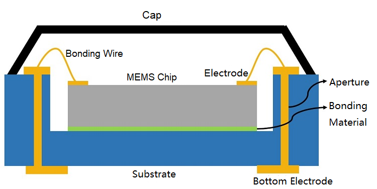
Figure 1. Schematic diagram of a typical MEMSchip scale package
Studies have shown that the die bond process is the main source of stress in chip scale packaging. The property mismatches of MEMS chip substrate materials, bonding materials, and packaging substrates create packaging stress, especially the CTE mismatch between the MEMS substrate silicon and the packaging substrates. Packaging stress can directly cause warpage and deformation of the chips, which in turn affects the performance of the MEMS devices. For some stress-sensitive MEMS devices, such as piezoresistive sensors and pressure sensors, the stress generated in the packaging process directly acts on the device itself, which directly affects the accuracy of its measurement results. For resonant devices or inertial devices, such as MEMS resonators, accelerometers, and gyroscopes, structural geometric deformation and equivalent stiffness changes due to package stress will change the resonant frequency and quality factor (Q) of the device. As a result, the output signal of the sensor, such as scale factor offset and zero offsets. When the stress on the device is high, it can cause cracks, delamination, or even failure of the MEMS devices in the interface area, destroying the interconnection of the MEMS devices and causing failure or long-term reliability problems.
Controlling and reducing package stress is important for improving the performance reliability and long-term stability of stress-sensitive MEMS devices such as pressure sensors, resonators, and inertial devices. Therefore, this article mainly focuses on the die bond process and analyzes the mechanism of packaging stress. At the same time, from the aspects of packaging materials, packaging processes, and packaging structures, the measures to reduce packaging stress and increase MEMS device reliability will be discussed. What’s more, a summary and prospect of MEMS device low-stress packaging technology are included.
1 Stress generation mechanism in chip bonding process
The die bond is a process in which the die is attached to the package substrate through an adhesive material. The process is generally divided into three steps, including solder addition, die patching, and curing. First, the MEMS chip is fixed to the package substrate through a bonding material. Then the overall structure is heated to the curing temperature, and finally, the chip is cooled to room temperature to complete the chip bonding. When cooling from the curing temperature to room temperature, the MEMS package structure is deformed due to residual thermal stress caused by material properties mismatch between the MEMS substrates, the bonding material layers, and the package substrates. The typical 3-layer structure made of the MEMS chip, the bonding material and the package substrate is shown in Figure 2.
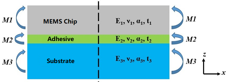
Figure 2. Typical three-layer structure in die attachment process
According to Suhir's theory, starting from the relationship between the bending moment and the bending curvature in the pure bending process, the solution of the package stress in the process of die bonding is deduced by numerical analysis. In this 3-layer structure, the thickness and mechanical properties of each layer determine the overall warpage or deflection w(x), which can be described by the following equations:

The shear stress τ0(x) in the die bond process can be accurately expressed as:

The peel stress σ0(x) during die bonding can be accurately expressed as:

Ei is Young's modulus of the i-th layer material; Gi is the shear modulus of the i-th layer material; vi is the Poisson's ratio of the i-th layer material; αi is the thermal expansion coefficient of the i-th layer material; The thickness of i-layer material; t is the total thickness of the multi-layer structure; Δα = α3 - α1, the difference between the thermal expansion coefficients of the chip and the package substrate material; ΔT = To - Tref, the difference between the working temperature To and the curing temperature Tref.
It can be seen from equations (1), (2), and (3) that the thermal stress of the package is proportional to the difference between the solidification temperature and the operating temperature during the cooling process and the difference between the CTE of the chip and the package substrate material. Meanwhile, the Modulus of elasticity, Poisson's ratio, and thickness are also related.
2 Low stress die bond
Based on the mechanism of packaging stress, in order to reduce the packaging stress in the MEMS packaging process, the current research mainly optimizes the packaging materials, packaging process, packaging structure, etc. Besides, researchers will introduce and analyze the low-stress die bond method for these three aspects.
2.1 Packaging material optimization
Differences in physical properties between the MEMS die materials, the bonding materials, and the substrate materials are a source of packaging stress. Therefore, the selection and optimization of packaging materials are beneficial to reduce packaging stress.
2.1.1 Bonding materials
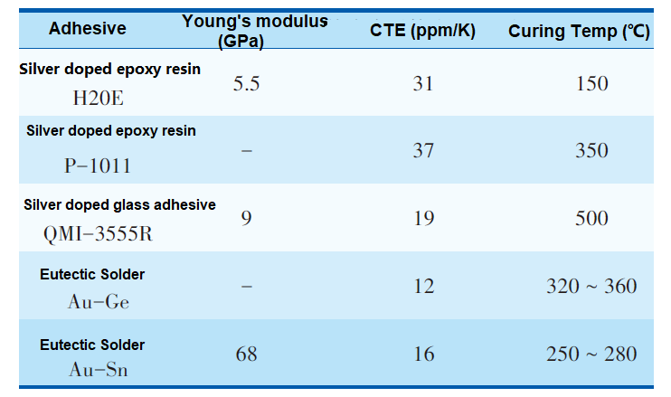
Commonly used die bond materials mainly include epoxy resins, eutectic solder pastes, and metal-doped glass adhesives. Epoxy resin is applied for low-temperature bonding of chips. Due to the poor thermal and electrical conductivity of epoxy resin, metal powder (such as gold and silver) is usually added to epoxy resin to improve the thermal and electrical conductivity of epoxy resin. However, eutectic solder pastes and metal-doped glass adhesive are mainly used for high-temperature bonding of chips, which are suitable for IGBTs. The bonding quality is good, but the cost is high. Table 1 shows the physical properties of some adhesive materials, from which the curing temperature of epoxy resin is lower than that of silver-doped glass adhesives and eutectic solders. The packaging stress caused by epoxy resin is smaller.
Table 1. Physical properties of some adhesive materials
Walwadka et al. studied the influence of Young's modulus and CTE of the bonding material in the die bond process on the die deformation caused by the package stress. The results show that the CTE of the bonding material has little effect on the packaging stress. The smaller the elastic modulus of the bonding material, the smaller the stress. Reducing the curing temperature and Young's modulus of the bonding material can significantly reduce the packaging stress of MEMS devices. Based on this, Königer et al. proposed an acrylate-based low-temperature curing method, which uses low Young's modulus low-stress bonding material with high bond strength. The Young's modulus of the new adhesive material is as low as 0.1GPa, and the curing temperature is reduced to 100°C, which effectively reduces the MEMS packaging stress. At present, companies such as Henkel in Germany, ZYMET, and EPOXY in the United States have developed epoxy resins for MEMS low-stress packaging, and low Young's modulus bonding materials have been commercialized. However, reducing the elastic modulus of the bonding material is only suitable for epoxy resin. The epoxy resin with low Young's modulus is not mixed with metal powder, so its thermal and electrical conductivity are poor, which makes it unsuitable for high-reliability packaging applications.

SAC Solder Paste SACS Solder Paste SnBiAg Solder Paste SnBiAgSb Solder Paste SnBiAgX Solder Paste SnBi Solder Paste BiX Solder Paste AuSn Solder Paste SnSb Solder Paste SnPb Solder Paste Anisotropic Conductive Paste Ultra-Fine-Pitch Flux

2.1.2 Substrate materials
The CTE difference between the packaging substrate material and the MEMS chip material is the main cause of packaging stress. Reducing the CTE difference between the substrate and chip can effectively reduce the packaging stress. The physical properties of the mainstream MEMS chip materials are shown in Table 2. Table 3 shows the physical property parameters of commonly used packaging substrate materials.
Table 2. Physical properties of commonly used MEMS chip materials
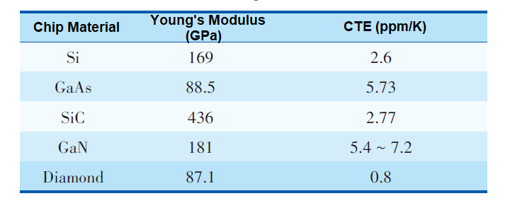
Table 3. Physical properties of commonly usedsubstrate materials
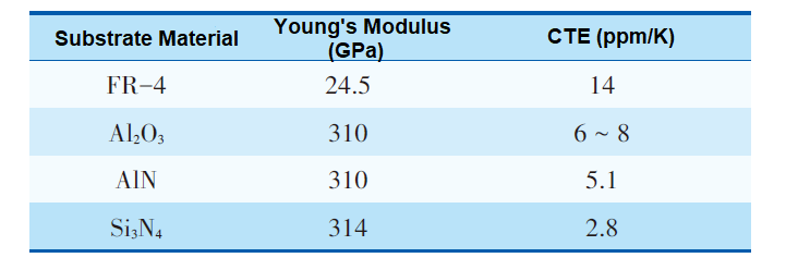
Sun et al. explored the stress on the surface of MEMS silicon chips during die bonding and curing of FR-4 (printed circuit board) substrates and Al2O3 ceramic substrates. The results are shown in Table 4. The packaging stress can be significantly reduced by using a ceramic substrate with a smaller CTE difference from silicon. A reasonable selection of packaging materials with CTE similar to MEMS chips can effectively reduce the packaging stress. However, in the actual development of MEMS devices, it is difficult to perfectly match the CTE of the packaging substrate materials and the MEMS chip materials. As a result, packaging stress is inevitable. In addition, packaging substrate materials with low thermal expansion coefficients are expensive and are not recommended for the commercial application of low-cost MEMS devices.
Table 4 Packaging stress under different substrate materials

2.2 Packaging process optimization
In the die bond process, the packaging stress is mainly generated during the solidification and cooling process. Optimizing the die bond process can reduce the packaging stress.
Frutschy et al. proposed a method for localized rapid heating of chips and bonding materials based on thermal pulse technology to reduce packaging stress. By controlling the power and time of the thermal pulse, the chip and the bonding material can quickly reach the curing temperature. Due to the short conduction time, the temperature of the substrate is relatively low at this time. The stress caused by the mismatch can be reduced accordingly. Figure 3 compares the chip warpage results obtained from the thermal pulse method and the traditional thermal curing process. It can be seen that when the heating time is less than 1s, the overall chip warpage is reduced by 50% compared with the traditional process method. This method can effectively reduce packaging stress, but its wide application is limited due to the complex process steps and high cost.
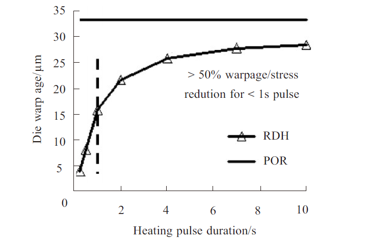
Figure 3. Comparison of chip warpage using traditional dieattachment and pulse laser heating bonding process
Walwadkar et al. proposed a thermal cycle curing process to reduce package stress. The adhesive material is silver glass adhesive. After the die bond process is completed, the chip structure is heat treated by thermal cycling (1-400°C). The experimental results show that the packaging stress decreases significantly during thermal cycling. The silver glass adhesive produces stress relaxation under thermal cycling, which reduces the stress of the package. However, this method is only suitable for silver glass bonding materials.
2.3 Package structure optimization
Optimizing the package structure is the most common method for reducing MEMS package stress. Optimizing the package structure can change the distribution and conduction of package stress, thereby reducing the impact of stress on MEMS devices. The packaging stress between the chip and the packaging material is mainly transmitted through the bonding material. Figure 4 shows the stress change on the top surface of the MEMS chip when the bonding area is changed in the simulation die bonding process. It can be seen that as the bonding area decreases, the packaging stress on the MEMS chip is smaller. Li et al. directly reduced the impact of packaging stress on the performance of MEMS accelerometers by reducing the bonding area. This low-stress packaging method has been successfully applied to the mass packaging of Motorola MEMS devices.
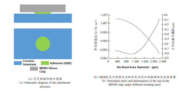
Figure 4. Simulated stress on the top surface of the chip under different bonding areas in die attachment
Prikhodko et al. studied the effect of package stress on the deformation and performance of MEMS gyroscopes when Au-Sn eutectic alloy solder was used for die bonding. The experiment compares the structural deformation of the gyro device after chip bonding in the two cases of full surface bonding and small bonding area (Figure 5). The beam structure of the device is clearly deformed under the whole-surface pasted structure (Figure. 5a). The structural deformation of the MEMS device after reducing the chip bonding area is shown in Figure 5(b). The beam structure of the MEMS gyroscope has almost no deformation. It shows that the shrinking of the bonding area can significantly reduce the stress and deformation of the MEMS device structure. At the same time, by reducing the bonding area of the gyroscopes, the frequency drift of the resonant gyroscope devices is reduced to 20%, which effectively improves the stability and reliability of the MEMS gyroscopes.
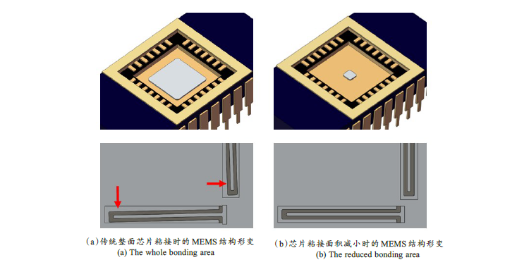
Figure 5. The structural deformation of MEMS devices induced by packaging stress under different bonding areas
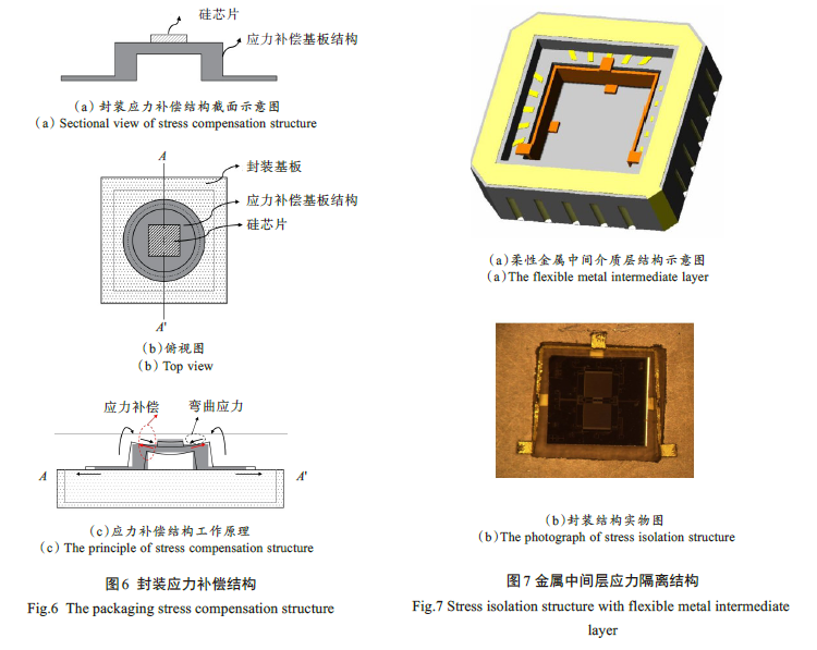
Samejima et al.from Yokogawa electric company proposed a substrate structure with thermal stress compensation for compensating the packaging stress of MEMS pressure sensors (Figure 6). The packaging structure is shown in Figures 6(a) and (b). The stress compensation structure is a substrate structure with a cavity. The working principle is shown in Figure 6(c). The silicon chip is bonded to the substrate of the thermal stress compensation structure. When the substrate structure is thermally expanded, the lower end of the thermal stress compensation structure is subjected to tensile stress, and the upper end is depressed. Compressive stress is generated at the lower end of the chip, which will offset the tensile stress caused by the thermal expansion of the chip. Similarly, when the substrate is cooled and contracted, the lower end of the thermal stress compensation structure is subjected to compressive stress, and the upper end of the thermal stress compensation structure protrudes at the lower end of the chip. The tensile stress will compensate for the compressive stress caused by the cold shrinkage of the chip, thereby reducing the stress. Under the traditional die bond process, the output error of the pressure sensor caused by the packaging stress is as high as 250 με/K, while the output error of the pressure sensor using the thermal stress compensation structure is reduced to 6 με/K. This method effectively reduces the influences of the packaging stress on the pressure sensor output error.
Marinis et al. used a flexible metal intermediate dielectric layer structure on the ceramic substrate to reduce the die bond stress. The structure is shown in Figure 7. The interlayer structure can reduce the thermal expansion mismatch between the chips and the ceramic substrates and play a role in stress isolation. Compared with the traditional bonding method, the chip warpage caused by stress is reduced by about five times when the flexible metal intermediate layer structure is added, and the stress caused by the bonding process is significantly decreased.
Schröder et al. proposed a double-sided wire-bonding method for low-stress packaging of MEMS gyroscopes. The method targets to replace the traditional die bond process with a double-sided wire bonding process. The MEMS chip leads out several metal leads through the packaging frame to achieve electrical conduction. At the same time, the upper and lower end faces of the MEMS chips are fixed. The method fixes the MEMS chips through wire points, and significantly reduces the bonding area with the substrate, which plays a good role in stress isolation. The deformation of the MEMS gyroscope chips caused by stress under the double-sided wire bonding method is significantly reduced, indicating that this method can effectively reduce the warpage of the chips caused by stress. By optimizing the number of bonding wires, this method can reduce the resonance mode of the MEMS gyroscope and the influence of the spurious modes on the performance of the MEMS gyroscopes. However, this method increases the complexity of the process and is not appropriate for large-scale batch manufacturing.
3 Conclusion
MEMS packaging involves many disciplines and fields, such as mechanics, materials, thermophysics, and electronic information. The unreasonable material selection, process, and packaging structure in the bonding process will lead to packaging stress. Packaging stress severely affects the stability and reliability of stress-sensitive devices such as MEMS pressure sensors, resonators, and inertial devices. At the same time, this article introduces the current methods of reducing packaging stress in the chip bonding process from the aspects of packaging materials, packaging technology, and packaging structure. There are still some limitations in the current method of reducing packaging stress, and low-stress packaging materials are only suitable for specific applications because the packaging process and structure are complex and expensive.
With the continuous development of MEMS device applications, the precision and stability requirements for stress-sensitive MEMS devices in the industry continue to increase. Low-cost and versatile low-stress packaging technology is challenging. The means of reducing packaging stress in the future mainly focus on two aspects. One is the research and development of new packaging materials. We should focus on developing low-stress adhesive materials with good versatility and packaging substrate materials that perfectly match the CTE of MEMS chip materials. The second is to further optimize the package structure, mainly focusing on the development of stress isolation structure and stress compensation structure. On this basis, it is necessary to specifically consider the structure and working principle of different types of MEMS sensors. Meanwhile, it is necessary to take into account the cost and complexity of the packaging method to propose a corresponding effective method for reducing stress.
Authors:吴忠烨,杨尚书,吴国强
(Wuhan University Industrial Science Research Institute)




 Back to list


