The Causes and Solutions of Pseudo Soldering
The Causes and Solutions of Pseudo-Soldering
Pseudo soldering is caused by the failure to form an effective intermetallic compound (IMC) layer during soldering, resulting in a less dense connection at the interface between the component and the substrate. It is hard to detect if solid solder joints are formed by eyes. From the microstructure view, it can be seen that the connection is not tight. The consequence of pseudo soldering is that the electrical connection becomes unstable, leading to an open circuit. With the influences of the external environment and long working time, pseudo soldering will become more serious.
1. Causes
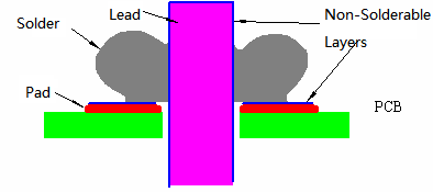
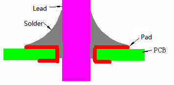
One of the reasons for the appearance of pseudo soldering is the improper use of solder. Insufficient solder paste is used when printing, resulting in an ineffective bonding between the component and the substrate. Many factors affect the amount of solder paste printed on the substrate, including printing speed and pressure, stencil aperture size and thickness, solder paste viscosity, printing angle, etc. Another important reason is that oxidation of impurities deposited on the surface of the soldered components will reduce solderability. The electrical resistance increases due to the oxidized layer and causes pseudo-soldering (Figure 1). In addition, temperature, humidity, and soldering time can also lead to pseudo-soldering. For example, too low soldering temperature and short soldering time can affect the diffusivity of tin. Hence, low soldering temperature and short holding time diminish the IMCformation (Figure 2). If the working environment is too humid, the performance of the solder paste will be affected. Moreover, the unstable and shaky printing platform will affect the soldering effect.

Figure 1: Non-solderable layer inhibits the metallugical connection bwtween the lead and solder

Figure 2: Insufficient solder fails for metallugical connection
2. Solutions
l Check the amount of solder paste on the stencil during printing: when the amount of solder paste on the stencil is less than one-third, it needs to be replenished in time.
l Avoid excessive solder paste residence time: The solder paste will dry out and affect the soldering performance if it stays on the stencil for a long time. It is recommended that the continuous printing time should not exceed 8 hours. Reflow soldering should be carried out in time after printing is completed. The preferably residence time of solder paste is no more than 4 hours.
l Maintain a slow printing speed: Controlling the printing speed can make the solder paste evenly and adequately cover the pads. Generally, the speed of the squeegee is 25mm/s. Squeegee speed is adjustable according to the aperture sizes and the types of solder paste.
l The most suitable ambient temperature and humidity for solder paste application are about 20-25℃ and 40-50%RH, respectively. Solder paste quality can be ensured by monitoring environmental conditions.
l The timely detection of component oxidation and organic contamination can avoid poor solder paste wetting during soldering. One way is to forego the use of oxidized components. Another method is to use a knife or mild acid to remove the oxide layer and contamination. However, this process is hard to implement because of the small component sizes.
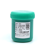
Fitech is committed to providing high-quality solder paste for semiconductor packaging. Fitech’s solder paste has excellent wettability, uniform particle size distribution, and stable viscosity, which can be used for printing with an excellent soldering effect.


 Back to list


