The Applications of 5G and Its Packaging Process
The Applications of 5G and Its Packaging Process
With the development of communication technology, users have higher requirements for the network performance and battery life of mobile phones. In this regard, many mobile phone manufacturers have recently developed 5G chips. The high integration of the chips dramatically accelerates the internet speed and stability, and the size becomes smaller and smaller. The chip size has reached 5nm. 3nm chips are under development. Not only mobile phones, but 5G also has excellent potential in the communication industry, AI, Internet of Things (IoT), and others.
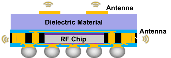
5G technology introduces the concept of millimeter-wave (mmWave). Compared with the Sub-6 frequency band, mmWave can provide a larger bandwidth and a communication speed several times faster. It is well known that wavelength and frequency are inversely proportional. Since a 5G mmWave requires high-frequency implementation, the wavelengths emitted by the antenna are extremely short, reducing the antenna size. However, shorter wavelengths are prone to interference and attenuation. Therefore, it requires more antennas for signal coverage. 5G mobile phones and automotive radars integrate a wide variety of RF components and antennas far exceeding 4G. The substrate size is only 30x30mm, and the line width and spacing are less than 20μm. The packaging of millimeter-wave antenna modules currently adopts AiP (Antenna in Package) technology. This package style can integrate front-end components, switches, filters, and other components through SiP technology to reduce the size, transmission distance, and power loss. TMYTEK considered three AiP fabrication technologies, including applying low-temperature co-fired ceramic (LTCC) and high-frequency PCB. Based on PCB, TMYTEK has developed AiP modules with multi-layer PCBs and realized 1x8 to 8x8 array products. Meanwhile, TMYTEK used LTCC with excellent electrical and packaging characteristics for AiP design and achieved significant results.

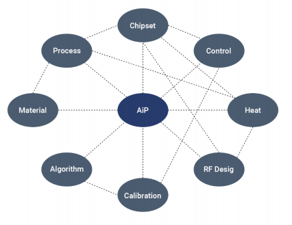
Figure 1: AiP Process

Figure 2: AiP Configuration
Fan-Out Wafer Level Packaging (FOWLP) is a new idea for achieving 5G packaging. FOWLP places the processed and diced chips in an epoxy mold and uses the RDL method to complete non-substrate packaging. RDLs can be routed in and out, enabling more I/Os, better cooling, and smaller size. TSMC's integrated fan-out packaging technology (InFO) has been practiced and applied.
Shenzhen Fitech can provide solders for 5G chip packaging. Welcome to contact and inquire.


 Back to list


