The Introduction of MEMS Packaging
The Introduction of MEMS Packaging
1. Introduction
MEMS is a system that connects micro-sensors, micro-actuators, signal processing, circuits, and other components together. It is mainly used for various types of sensors. After a long-term study of IC packaging, it was decided to extend the practice of IC packaging into MEMS. Although many MEMS packaging methods are extensions of IC packaging, the high complexity of MEMS increases the packaging difficulty and cost. In general, the cost of MEMS packaging accounts for half or more of the total equipment cost because there is no standard packaging technology due to the uniqueness of MEMS. Conventional IC packaging needs to provide a reasonable chip pin distribution and can achieve electrical connections. The difference between the IC and MEMS packaging is that the MEMS packaging shell should provide channels for the transfer of various energies and media, such as optical signals, electrical signals, fluid components, etc., which increases the difficulty of packaging.
2. MEMS Pakcaging Requirements
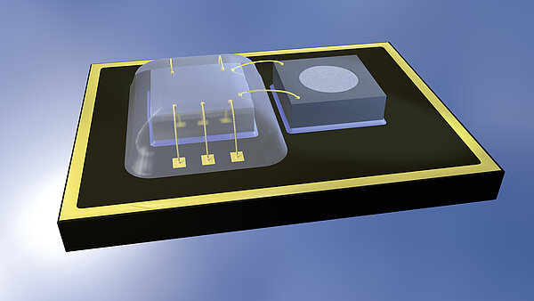
Due to the transfer requirements of signals and media, MEMS inevitably have to come into contact with the external environment. The small size of MEMS chips makes them easily affected by the impurities in the application environment. It may corrode the components and affect their reliability. In addition, vibration, shock, and temperature changes generated during packaging will affect the reliability and performance of components with fragile mechanical structures. The stress generation should be reduced to ensure high-precision sensors. The internal circuitry needs to be effectively isolated from the external environment. MEMS tend to be non-removable for cleaning. Hence, the volatiles residue can affect the component reliability that should remain in a small range. The packaging effect is shown in the figure below.

Figure 1:MEMS Packaging Effect
3. MEMS Packaging Processes
Compared with wire bonding, a new type of flip-chip packaging technology has been explored. Flip-chip is a technology that flip-chips a chip on a substrate. It significantly increases the I/O density. Besides, the flip-chip avoids signal interference caused by wires. Single-chip/multi-chip packaging and wafer-level packaging (WLP) can adopt the flip-chip method. To maintain high precision, the MEMS packaging is usually under a vacuum condition.
① Single-chip/Multi-chip packaging
Chip-scale packaging is the packaging of chips after being removed from a wafer. The majority of substrates used are ceramic or glass. The MEMS chips and ceramic substrates require to process separately. The MEMS chip is connected to the substrate by SMD, wire bonding, or flip-chip. The chip is soldered to the ceramic substrate and capped. Common capping materials include metal, ceramic, etc. The purpose of the cap is to bring high airtightness and chip reliability.
② Wafer-Level Packaging
Wafer-level packaging is a technique of packaging on a complete wafer. The packaging processes include the polymer coating to the passivation layer of the wafer, rearrangement of wire layer in the soldering area, second layer coating, addition of under bump metal, and performing ball mounting. After packaging and testing, the wafer is diced to get several finished chips. The chips are soldered on the substrate using the flip-chip method after performance testing. Solder paste is used in this process. Finally, the chip should interconnect with caps through various bonding processes before dicing.
Currently, these two packaging methods still have defects. However, wafer-level packaging is undoubtedly the mainstream of MEMS packaging with the evolution of technology. Manufacturers have gradually developed different branching routes of wafer-level packaging.


 Back to list


