T8 Lead-Free Solder Paste for MEMS Package:STMicroelectronics' 500,000 Megapixel 3D ToF Sensor
T8 Lead-Free Solder Paste for MEMS Package:STMicroelectronics' 500,000 Megapixel 3D ToF Sensor
Solder Paste and Ultra-Fine Solder Manufacturer-Shenzhen Fitech is a comprehensive solder paste supplier integrating production, sales, research, and service of solder paste, epoxy solder paste, and solder powder. Fitech is the leading unit for the formulation of solder powder standards of the Ministry of Industry and Information Technology. Fitech's products include ultra-fine lead-free printing solder paste, ultra-fine lead-free dispensing solder paste, ultra-fine lead-free jetting solder paste, ultra-fine lead-free pin transfer solder paste, no-clean solder paste, water-soluble solder paste, high-temperature solder paste, medium-temperature solder paste, low-temperature solder paste, etc. Fitech can manufacture electronic-grade packaging solder powders with particle sizes from T2-T10.

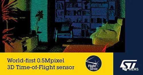
3D time-of-flight (ToF) sensors enhance the 3D imaging and sensing performance in smartphones, AR and VR devices, and consumer robots.
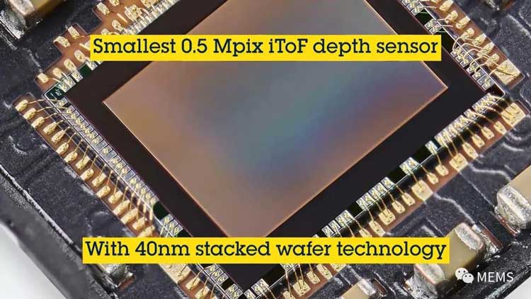
40nm stacked wafers are based on proprietary indirect time-of-flight (IToF) back-illuminated (BSI) technology with low power consumption, small size, and high performance.

STMicroelectronics, a global semiconductor industry leader, recently announced the launch of a new high-resolution 3D ToF VD55H1 series that would bring more advanced 3D imaging and sensing capabilities to devices such as smartphones.
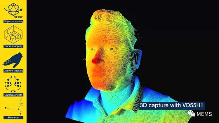
The VD55H1 sensors map 3D surfaces by measuring distances of 50.5 million points. It can detect objects up to 5 meters away and even further detect through patterned lighting. The VD55H1 sensors easily address the applications in emerging AR/VR markets, including room mapping, gaming, and 3D virtual imagery. The VD55H1 sensors can significantly improve the performance of camera systems, including virtual background effects, multi-camera selection, and video segmentation. Higher-resolution and accurate 3D images can also improve the security of face authentication, protecting mobile phone unlocking, mobile payments, and any smart system involved in secure transactions and access control. In the field of robotics, the VD55H1 sensors can provide high-fidelity 3D scene mapping for more powerful and novel functions.

The applications of VD55H1 Sensor
The innovative VD55H1 sensor reinforces STMicroelectronics' leading position in the ToF field and is a good complement to the entire range of depth sensing technologies. Ericausedat, executive vice president of STMicroelectronics, said the Flightsense product portfolio includes direct time-of-flight (DToF) and IToF products, including single-point ranging multifunction sensors and complex high-resolution 3D imaging sensors.
IToF sensors such as VD55H1 calculate the distance between the sensor and the object by measuring the phase difference between the reflected signal and the transmitted signal, which is a powerful complement to the DToF technology. The DToF sensors directly measure the time required for the transmitted signal to reflect back to the sensors. The advanced STMicroelectronics technologies enable it to design and deliver the two kinds of ToF technologies and provide customized solutions according to application requirements.

SAC Solder Paste SACS Solder Paste SnBiAg Solder Paste SnBiAgSb Solder Paste SnBiAgX Solder Paste SnBi Solder Paste BiX Solder Paste AuSn Solder Paste SnSb Solder Paste SnPb Solder Paste Anisotropic Conductive Adhesive Ultra-Fine-Pitch Flux


VD55H1 sensor for 3D face imaging.
The VD55H1 sensor adopts independent 40nm stacked wafer technology to realize a unique pixel structure and manufacturing process, ensuring low power consumption, low noise, and optimized chip area. The VD55H1 sensor offers 75% more pixels than existing VGA sensors with a smaller chip size (4.5mx4.9mm).
The VD55H1 sensor is available to send samples to key customers. Mass production is expected in the second half of 2022. STMicroelectronics provides a reference design and complete software package to accelerate the evaluation and project development progresses of 3DTOF sensors.
More technical information.
The VD55H1 sensor uses a 672x804 back-illuminated (BSI) pixel array for IToF depth sensing, which ranks top one in the industry.
The VD55H1 is a IToF sensor chip with low noise, low power, and 672x804 pixels (0.54 mpixel) manufactured using advanced back-illuminated stacked wafer technology. The integrated 940nm lighting system can construct a small 3D camera and provide a high-definition depth map. The typical full-resolution detection distance reaches 5m, and the pattern lighting detection distance can achieve more than 5m.

The VD55H1 is the world's smallest 500,00 megapixel IToF depth sensor.
VD55H1 sensor's depth accuracy is twice that of typical 100mHz modulation sensors. It has a unique ability to operate at 200mHz modulation frequency and reach a demodulation contrast ratio of over 85%. At the same time, multi-frequency operation provides long-distance detection. Low-power 4.6μm pixels provide optimal power performance. In some modes, the average power consumption of the sensor can be as low as 80mw.
The VD55H1 sensor outputs 12-bit raw digital video data through MIPICSI-24-channel or dual-channel interface with a clock frequency of 1.5gHz. Its frame rate can reach 60fps at full resolution and 120fps in emulated bing2x2. STMicroelectronics has developed an exclusive software image signal processor (ISP) that converts raw data into depth maps, amplitude maps, confidence maps, and offset maps. In addition, it supports Android formats such as DEPTH16.
The VD55H1 sensor is fully configurable via the I2C serial interface. It has a 200mHz low dropout signal (LVDS) and a 10mHz three-wire SPI interface for highly flexible control of the laser driver. The sensor is also optimized for low EMI/EMC, multi-device immunity, and calibration procedures.
Source: MEMS, retrieved by Fitech


 Back to list


