01
More transistors per unit area

Solder Paste and Ultra-Fine Solder Manufacturer-Shenzhen Fitech is a comprehensive solder paste supplier integrating production, sales, research, and service of solder paste, epoxy solder paste, and solder powder. Fitech is the leading unit for the formulation of solder powder standards of the Ministry of Industry and Information Technology. Fitech's products include ultra-fine lead-free printing solder paste, ultra-fine lead-free dispensing solder paste, ultra-fine lead-free jetting solder paste, ultra-fine lead-free pin transfer solder paste, no-clean solder paste, water-soluble solder paste, high-temperature solder paste, medium-temperature solder paste, low-temperature solder paste, etc. Fitech can manufacture electronic-grade packaging solder powders with particle sizes from T2-T10.

Introduction
All exponentially growing curves are physically unsustainable, including Moore's Law.
However, People have made efforts to continue Moore's Law. Why do they know they can't do it? This represents human idealism. This ideal or belief often enables humans to surpass themselves and create unexpected technologies and civilizations.
Perhaps it is the belief in the sustainability of Moore's Law that has fueled the rapid development of integrated circuits for over 50 years. When Moore's Law was proposed, I don't think Moore himself believed that a chip could integrate more than 100 million transistors.
Today, there are more than 10 billion integrated transistors on a chip with fingernail size. Can there be more transistors? The answer remains yes.
However, with the extreme (3nm~1nm) chip characteristic size, the scaling of transistor size in integrated circuits is approaching the physical limit of silicon atoms. The width of 1nm can only accommodate two lattices of silicon atoms (a=0.5nm), representing that the side-by-side width of three silicon atoms is 1nm.
What will be the development direction of IC technology in the future? You may find your answer in this article.

01
More transistors per unit area
The development of modern technology is based on integrated circuits. The most direct goal of integrated circuit development is to integrate more transistors per unit area or per unit volume. Therefore, the first development direction is to include more transistors.
More transistors per unit area
Integrating more transistors per unit area requires smaller transistors. Driven by Moore's Law for decades, the feature size of transistors has been reduced by a million times from millimeters to microns to nanometers. Nowadays, more than 100 million transistors can be integrated into one square millimeter, and the number of transistors on a chip has reached tens of billions.
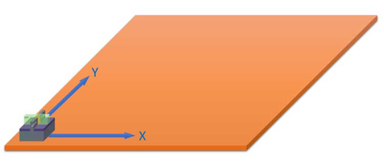
More transistors per unit area
How small can transistors reach? The size is roughly constrained by two factors. One is the minimum structure width within the transistor, and the other is the area occupied by the transistor.
The smallest structure width of a transistor, usually the gate width, was 22nm before called the feature size. With the shrinking of the transistor area, the feature size and manufacturer naming are gradually different. The gate width is no longer the minimum structure width of the transistor. For example, in FinFET, the width of Fin is usually smaller than the gate width. In GAA stacked nanosheet transistors, the thickness of the nanosheet is smaller than the gate width.
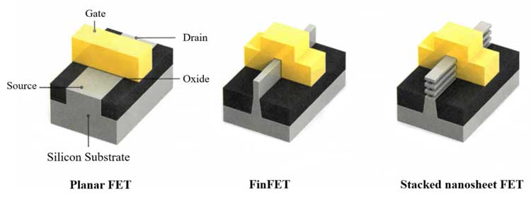
Therefore, foundries no longer use gate width as the feature size of transistors. The process node has become a synonym, which does not correspond to a specific width, but still has its physical meaning. It is reflected in the transistor area reduction, and more transistors can be integrated into the same area.
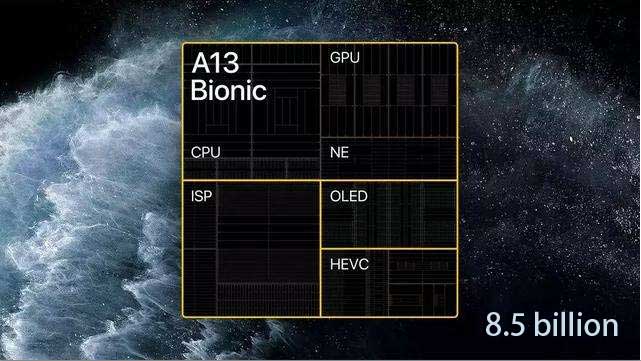
For example, the Apple A13 chip adopts a 7nm process with 8.5 billion transistors and an area of 94.48 square millimeters. It can integrate 89.97 million transistors in 1 square millimeter, equivalent to 0.8997 billion/mm^2. The Apple A14 chip adopts a 5nm process and has 11.8 billion transistors with an area of 88 square millimeters. The A14 chip can integrate 134 million transistors in 1 square millimeter, equivalent to 134 million/mm^2.
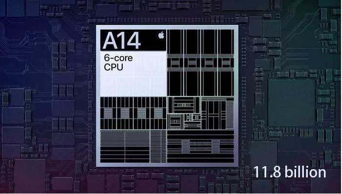
The ratio of the average area of the two transistors is 1.49. If the dimension ratio of 7:5 strictly obeys 1.4, the square will be 1.96. It can be seen that compared with the 7-nanometer chip, the 5-nanometer chip achieves 76% of the theoretical value. It is the reason why intel has always thought that the product naming by other foundries is biased.
From planar transistors to FinFETs to GAAs, the size of transistors has been shrinking, and the structure has been optimized to integrate more transistors per unit area.
More transistors per unit volume
By integrating more transistors per unit volume, the transistors become smaller and can be stacked because of an additional spatial dimension.
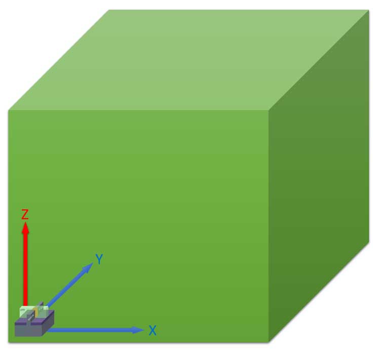
More transistors per unti volume
How to stack transistors?
There are two methods. The first is to directly manufacture transistors into multiple layers on the wafer through a special process. The other is to make a layer of transistors on the wafer in the same way as the traditional process and then stack multiple wafers. The wafers are connected by TSV.
Regarding the first method, there is a lot of research, such as stacking NMOS on PMOS. It saves half the area and doubles the transistor density. The difficulty is that the transistors in the upper layer are not supported by a dense silicon substrate. Therefore, it is hard to produce high-quality transistors. Additionally, the current technology only supports two-layer stacking.

The second method is currently popular and is often referred to Advanced packaging.
Advanced packaging, also known as HDAP high-density advanced packaging, is currently attracting a lot of attention. The technology is developing rapidly, allowing a higher interconnecting TSV density and more stacked layers. The most advanced technology belongs to Foundry.

However, foundries regard it as an important part of wafer manufacturing, such as TSMC, which defines it as 3D Fabric in its product line.
In theory, the three dimensions of XYZ are not fundamentally different. Therefore, if one dimension is added, the number of integrated transistors may increase thousands of times, which is considered an important reason for the sustainability of Moore's Law.
In integrated circuits, transistors are the smallest functional unit. We can call them functional cells. Integrating more functional cells per unit volume increases the functional density of the system.
From a historical point of view, in all man-made systems, the functional density is constantly improving. Although technology has increased rapidly or slowly at different historical stages, it will not stagnate in the development of human civilization.

SAC Solder Paste SACS Solder Paste SnBiAg Solder Paste SnBiAgSb Solder Paste SnBiAgX Solder Paste SnBi Solder Paste BiX Solder Paste AuSn Solder Paste SnSb Solder Paste SnPb Solder Paste Anisotropic Conductive Adhesive Ultra-Fine-Pitch Flux

02
Expanding silicon element
Although compound semiconductors are relatively popular, silicon occupies an absolute mainstream position in integrated circuits. Therefore, chip makers have been trying to apply compound semiconductors to conventional silicon wafers, making efficient use of existing resources to create greater economic benefits.
GaN-on-silicon
More efficient power technology is achieved by integrating GaN-based power devices with silicon-based CMOS on a 300mm silicon wafer. It allows the CPU to operate with low-loss and high-speed power delivery, meanwhile reducing motherboard components and space.
GaN semiconductor devices can be mainly divided into GaN-on-Si, GaN-on-SiC, GaN-on-sapphire, etc.
Due to restriction factors such as cost and technology, GaN-on-silicon has become the mainstream of the current semiconductor market.
Intel has firstly integrated GaN-based power devices on 300mm silicon wafers. This study verifies the feasibility of the 300mm process. This method is more suitable for high voltage applications, increasing functions and improving mass manufacturing possibility.
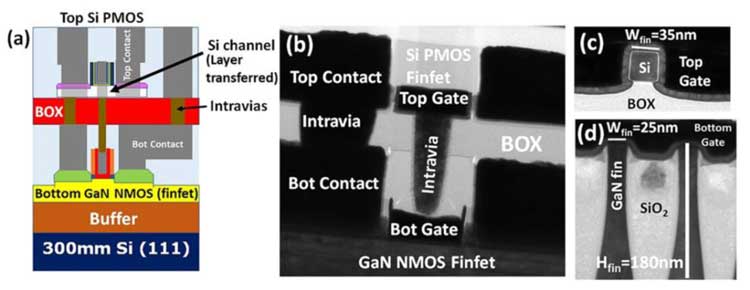
There are probably trillions of dollars of investment globally in 300mm silicon wafer equipment and ecosystems, which need to be fully utilized to reduce manufacturing costs.
In addition, TSMC is currently adopting GaN-on-Si technology.
Noval ferroelectric material
Another technology is the use of novel ferroelectric materials as a viable option for next-generation embedded DRAM technology. This technology can provide more memory resources and low-latency read and write capabilities to solve the increasingly complex problems in artificial intelligence and high-performance computing applications.
The ferroelectric memory adopts new technology to achieve a read and write speed of 2 nanoseconds and a read and write cycle of more than 10 to the 12th power. The ferroelectric memory’s performance and life are far beyond the existing memory.

Ferroelectric memory can be combined with the traditional CMOS process as an intermediate layer between L1 Cache and DRMA.
Good progress has been made in expanding silicon elements and improving the performance of silicon-based semiconductors in the fields of power devices and memory gain. People are making efforts to find other ways to expand silicon.
03
Exploring quantum realm
Due to quantum mechanical tunneling, electrons can travel through insulators, which would render the element ineffective. The researchers began for a new type of transistor that could further improve the performance of future integrated circuits to replace the traditional transistors. There is a lot of research, but there is still no substitution for silicon MOSFETs.
The researchers listed a range of MOSFET alternatives, including tunnel field effect transistors (TFETs), carbon nanotube field effect transistors, and single-atom transistors.
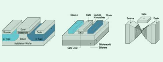
Tunnel field effect transistors (TFFT)
TEFT, different from traditional MOSFET transistors, has different source and drain doping. It uses quantum mechanical tunneling, where the voltage between the gate and source determines whether charge carriers can "tunnel" through the energy barrier between the source and drain and whether current is likely to flow.
According to quantum theory, some electrons can do this even though they obviously lack enough energy to overcome the energy barrier known as quantum tunneling.
In a TEFT, two small trenches are separated by an energy barrier. In the first slot, a large group of electrons waits silently, AND the transistor is not activated. When a voltage is applied, the electrons pass the energy barrier and move into the second trench, activating the transistor at the same time. TFETs are structurally similar to conventional transistors but adopt quantum mechanical tunneling in switching, which is energy efficient and fast.
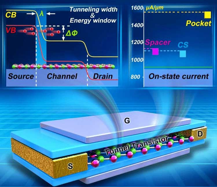
By reducing the magnitude of the energy barrier, it will be possible to enhance and exploit quantum effects. The energy required for electrons to pass through the barrier will be greatly reduced, and the power consumption of the transistor will drop significantly. The TEFT developed by using the quantum tunneling effect is expected to reduce the power consumption of the chip to one percent of the original value.
Carbon nanotube field effect transistors
Carbon Nanotube Field Effect Transistor (CNFET)
In CNFETs, the channel between the source and drain is composed of carbon nanotubes with a diameter of only 1–3 nm, which means that the channel is easier to be controlled by the gate. Therefore, carbon nanotube transistors have a greater potential for scaling down than conventional silicon-based transistors.
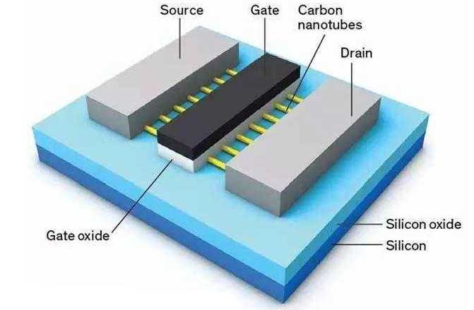
Carbon nanotubes have ultra-high room temperature carrier mobility and saturation velocity. At room temperature, the carrier mobility in carbon nanotubes is about 100 times that of silicon, and the saturation velocity is about 4 times that of silicon. Under the same channel length, the higher the carrier mobility, the higher the saturation velocity and speed. Moreover, it can increase energy utilization efficiency.
Carbon nanotube transistors have the potential for ultra-low voltage driving with low power consumption. For the selection of channel materials, carbon nanotube channels have a small size, better size reduction potential, and low power consumption.
Single-atom transistors
A single-atom transistor controls the electrode to move an atom that can connect the tiny gap between the two ends, allowing current to flow. In principle, it works like a relay with two steady states.
For a single-atom transistor, a single atom is moved by a voltage between the source and gate, enabling the closing or opening of the circuit between the source and drain.
Creating a tiny metal contact between gaps that is only a single metal atom wide is the smallest possible limit for current transistors. In this gap, a single atom is moved by electronically controlled pulses to complete the circuit closure. Moving the atom out of the gap can cut off the circuit
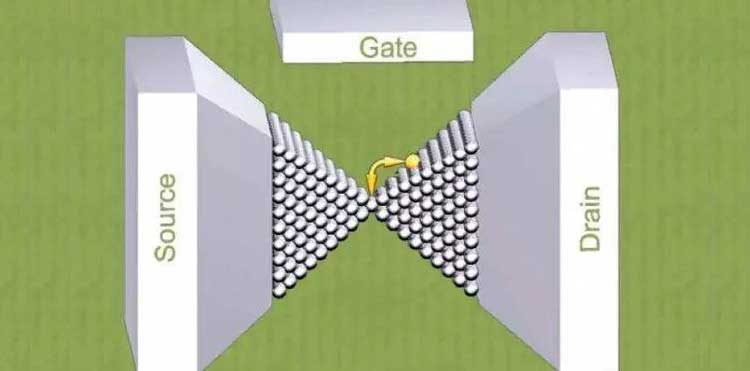
It enables the controlled reversible motion of individual atoms in the world's smallest transistor when power is on.
Single-atom transistors made of metal and free of semiconductor materials require extremely low voltages and power consumption. It was claimed that the energy consumption of a single-atom transistor would be only one ten-thousandth (1/10,000) of that of a traditional silicon-based transistor.
Unlike conventional quantum electronic components, single-atom transistors do not need to operate at low temperatures close to absolute zero. Single-atom transistors can operate at room temperature, which is a decisive advantage for future applications.
Source: SiP and Advanced Packaging Technoloy, retrieved by Fitech

CMOS image sensors arguably bring innovation to modern 3D imaging, even in the nascent lidar market. Flash solid-state lidar consists of many SPADCMOS sensors. Some manufacturers producing consumer im
2022-03-01Over the past 40 years, the era of PCs and mobile devices transited to the era of the cloud. Almost every aspect of our lives is stored and managed online. According to ASML’s...
2022-02-28The growing demand for lighting products has contributed to the expansion of the lighting LED packaging market. At present, LED lighting packaging products on the market include SMD and COB products.
2022-02-25In recent years, cross-border car manufacturing, new energy vehicles, and autonomous driving technology have become buzzwords in the business. The rapid rise of the automotive industry and the...
2022-02-24Silver is widely used in electrical connections and electronics because of excellent electrical conductivity, heat transfer, solderability, and low contact resistance. However, silver is the metal...
2022-02-23