Packaging Solder Paste: ASML’s Forecast of the Semiconductor Industry
Packaging Solder Paste: ASML's Forecast of the Semiconductor Industry
Solder Paste and Ultra-Fine Solder Manufacturer-Shenzhen Fitech is a comprehensive solder paste supplier integrating production, sales, research, and service of solder paste, epoxy solder paste, and solder powder. Fitech is the leading unit for the formulation of solder powder standards of the Ministry of Industry and Information Technology. Fitech's products include ultra-fine lead-free printing solder paste, ultra-fine lead-free dispensing solder paste, ultra-fine lead-free jetting solder paste, ultra-fine lead-free pin transfer solder paste, no-clean solder paste, water-soluble solder paste, high-temperature solder paste, medium-temperature solder paste, low-temperature solder paste, etc. Fitech can manufacture electronic-grade packaging solder powders with particle sizes from T2-T10.
Introduction
Recently, ASML released its 2021 annual report. Let's talk about the highlights and topics.
Over the past 40 years, the era of PCs and mobile devices transited to the era of the cloud. Almost every aspect of our lives is stored and managed online. According to ASML’s CTO Martin Vandenbrink, the next step in digitalization will be distributed intelligence driven by the seamless integration of communication, computing, and artificial intelligence. All of these trends require higher computing capability, which in turn accelerates the need for much more powerful and energy-efficient microchips.
With the continuous development of chip technology, chip manufacturing has become more complex. Based on the logicn5 node (5nm), the advanced processors contain billions of transistors. The next generation of chip designs will include more advanced materials, new packaging techniques, and complex 3D designs.
Lithography is the driving force behind making chips more capable and cheaper. ASML has always targeted to reduce the critical dimensions of chip processes. Its overall lithography product portfolio (EUV, ARFi, ARF, KRF, i-line systems, etc.) helps optimize production and reduce cost by integrating lithographysystems and matching computational modeling, measurement, and testing solutions.
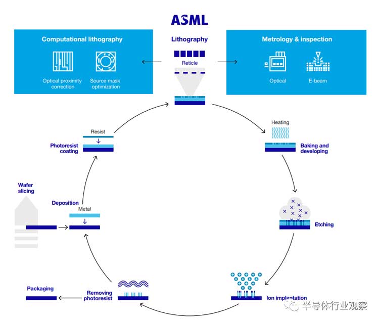
Semiconductor manufacturing process (from ASML)
The resolution of the lithography system is one of the main drivers of lithography shrinkage. It is mainly determined by the wavelength of light and the numerical aperture of the optical system. Shorter wavelengths are just like a thinner brush that can print smaller features. A larger numerical aperture can focus light more tightly and display better resolution.
The ASML lithography systems are developed by reducing wavelength and increasing value aperture. Over the years, ASML has made several wavelength steps from 365nm (i-line), 248nm (KRF) to 193nm (ARF). The EUV lithography machine has a wavelength of only 13.5nm.
NA is the numerical aperture of the optical system representing the incidence angle of light. Smaller structures can be printed by larger NA lenses. In addition to larger lenses, ASML also increases the NA of ARF systems (so-called immersion systems) by maintaining a film of water between the last lens element and the wafer. After the wavelength enters EUV, ASML has started to develop a next-generation EUV system called EUV0.55NA (HighNA), which increases the numerical aperture from 0.33 to 0.55.
TWINSCANXE:3600D is ASML's latest generation of EUV0.33NA lithography system. Compared with the predecessor TWINSCANXE:3400C, it can improve 15% to 20% productivity and about 30% coverage, supporting EUV mass production of 5nm and 3nm logic nodes and leading DRAM nodes.
The annual report states that the EUV product roadmap will help ASML achieve reasonable expansion of equipment prices over the next 10 years. The ASMLEUV0.33NA platform extends the customer logic and DRAM roadmap. Using EUV to manufacture chips reduces critical lithography modulus by 40% and process steps by 30%, significantly reducing cost and cycle time.
Data shows that since the launch of EUV, ASMLEUV lithography machines have produced more than 59 million wafers by the end of 2021, while 26 million wafers were created by the end of 2020. It can be seen that the EUV lithography machine is currently in the stage of rapid start-up. ASML expects EUV usage to continue to grow. By 2024, all advanced node chipmakers are expected to use EUV in production.
The next-generation EUV0.55NA platform will continue to enable efficient economic expansion for future nodes. The novel optical design of the new value aperture is developed to reduce the chip size by a factor of 1.7, further improve the resolution, and increase the microchip density by a factor of 3. The first early access system for the EUV0.55NA platform is expected to be operational in 2023. Customers are expected to start R&D in 2024-2025 and enter mass production in 2025-2026.
A lithography system is essentially a projection system that projects light onto the pattern to be printed (called a mask). The system's optics contract and focus the pattern on the photosensitive silicon wafer by encoding the pattern in the light. After the pattern is printed, the system gently moves the wafer and makes another copy on the wafer.
This process repeats until the wafer is covered by the pattern. To produce a complete chip, this process should be repeated layer by layer, superimposing patterns to form an integrated circuit (IC). Currently, the most simple chip has around 40 layers, and the more complex chips are over 150 layers.
Currently, DUV lithography systems are still mainstream in the industry. DUV systems support many market segments and are responsible for printing the majority of layers in customer devices. It will remain important in future devices.
DUVs currently used in the semiconductor industry are divided into immersion and dry lithography solutions. The i-line wavelength, KRF wavelength, and ARF wavelength are 365nm, 248nm, and 193nm, respectively, which is beneficial to manufacturing a wide range of semiconductor nodes and technologies, supporting industry cost and energy-saving expansion.
ASMLDUV immersion and dry systems lead the way in productivity, imaging, and coverage performance. It can combine EUV technology to produce leading logic and memory chips and continues to provide value for mature nodes and small applications.
ARF immersion lithography maintains a water film between the lens and wafer to increase NA and resolution, supporting further shrinkage. The ASML immersion system is suitable for single exposure and multi-pattern lithography and can be seamlessly combined with EUV systems to print the same chip. TWINSCANXT: The 2050i is the most advanced ASML immersion system currently applied in mass production at 5nm logic and fourth-generation 10nm DRAM nodes.
However, not every layer on a chip requires the latest and greatest immersion lithography system. Advanced or complex layers can be printed with advanced lithography systems, but other layers can be printed with conventional technologies such as dry lithography systems. The ASML dry system product portfolio provides customers with economical solutions with various wavelengths.
TWINSCANXT: 1470 is the ASML's latest dry ARF lithography system, providing a record productivity of 300 wafers per hour with 4nm coverage. TWINSCANXT: 86ON is a new generation KRF system with a resolution of 0.80NA, supporting the manufacture of large-volume 200mm and 300mm wafers with resolutions below 110nm. 0.93NATWINSCANXT:1060K is the most advanced KRF lithography system.
ASML’s CEO Peterwerwenink said that the industry market growth not only exists at the most advanced nodes but also requires mature lithography to manufacture many distributed computing and storage solutions. It is expected that by 2025, two-thirds of the total ASML system sales will be EUV, and the rest will be DUV and measurement inspection systems. This forecast is lower than the expectation in 2018, but this does not mean a contraction in the EUV market. It is clear that a growth period emerges in the DUV and measurement inspection market
The driving forces of semiconductor development in the future.
What is the pattern of the semiconductor industry? What are the key trends driving current and future industry development?
ASML believes that consumer demand, global competition for talent, geopolitical factors, expanding R&D investment, the changing external environment, and climate change are reshaping the semiconductor industry model.
Growing consumer demand: Wireless communications, telecommunications, media, and the cloud continue to fuel the global demand for advanced semiconductors. Growing population and urbanization are increasing the demand for advanced consumer electronic devices. Chips are the heart of these devices, and the continuous development and demand for emerging technologies are becoming an important driver of chip growth.
Global talent competition: High-skilled talent with technical backgrounds is scarce in the labor market, so competition is intensifying. Industrial companies are trying to increase human resources, but the high-tech talent is insufficient. The industry is competing for a small number of scientists, engineers, and software developers with the skills to develop and innovate solutions. The global talent competition is becoming increasingly critical. The number of STEM jobs is expected to increase dramatically, but filling these positions is challenging due to the lack of qualified candidates. Retaining talent has become the key for tech companies.
Global Geopolitics: The current trade environment presents significant challenges for the global semiconductor industry. The rise of trade tensions and protectionism is likely to continue. The global virus outbreak has reminded governments globally that global supply chains can have significant geographic dependencies on services, raw materials, and products.
Semiconductors play an increasingly important role in the growth and continuity of large industrial complexes. The government has turned its attention to the semiconductor supply chain to ensure adequate supply and plans to invest massively in the semiconductor industry. According to external data, the United States, China, the European Union, Japan, and South Korea are expected to nearly double their annual capital expenditures to $150 billion in 2021. In addition to the financial impact, trade tensions and protectionism have created great complexity in the entire supply chain and its processes, forcing the industry to re-examine the global supply chain.
Expanding R&D investment: Chip design and manufacturing technologies are the competitive basis for the rapid development of the semiconductor industry. Chipmakers face increasingly complex supporting applications and end markets. Meanwhile, traditional semiconductor companies are challenged by diversifying portfolios as tech platform companies move toward internal chip design.
Besides, the incremental cost of innovation is rising, requiring higher levels of R&D investment to achieve the same goals. Getting products to market faster is critical, or opportunities pass by. As a result, the pressure on quick solution provision to customers is increasing.
Changing environment: To take advantage of the integration of AI, IoT, 5G, and autonomous vehicles, the industry invests in assets that unlock value across the entire portfolio.
In recent years, the global semiconductor industry has shown a huge growth trend and is expected to continue. The industry focuses on technology and markets to enhance its core competencies. Acquisitions and joint ventures are expected to be key components of the chip market strategy.
Take action on climate change: Climate change is a globally pressing issue. The semiconductor manufacturing process consumes a lot of energy and water. As Moore's Law progresses, increasing chip computing power and storage capacity will increase the demand for these resources. To improve the efficiency of energy and water usage, new devices and ways of looking at the entire ecosystem are needed. In order to overcome the challenges, the semiconductor industry must reduce power consumption.
In this regard, ASML mentions that due to the versatility, innovation, production, maintenance speed, and cost-effectiveness of DUV and EUV platforms. ASML is investing in the energy efficiency of its products to help reduce the energy required for wafer production. Furthermore, ASML has a roadmap dedicated to reducing waste and working with customers and suppliers to reuse parts, tools, and packaging as much as possible across its value chain to prevent unnecessary waste.
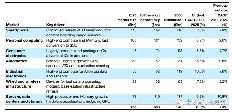
In addition, judging from ASML's outlook on the current market size and market opportunities of the entire industry, the driving factors of different segmented application markets are shaping the model of the semiconductor industry, becoming the main trend promoting the development of the industry at present and in the future.

SAC Solder Paste SACS Solder Paste SnBiAg Solder Paste SnBiAgSb Solder Paste SnBiAgX Solder Paste SnBi Solder Paste BiX Solder Paste AuSn Solder Paste SnSb Solder Paste SnPb Solder Paste Anisotropic Conductive Adhesive Ultra-Fine-Pitch Flux

 What are the reasons behind the ASML revenue increase?
Market demand for advanced mature nodes grew driven by global chip shortages, accelerated digital infrastructure, and technological sovereignty. In 2021, ASML's net sales reached a record 18.6 billion euros that increase of 4.6 billion euros from the previous year.
Rogerdassen said logic system sales rose by 2.2 billion euros, or 30% in 2021, due to strong customer demand for mature nodes. Memory system sales increased by 1.1 billion euros and 39% due to high end-market demand for servers and smartphones.
The increase in net sales was driven by demand from ASML across all technologies. In 2021, ASML successfully shipped 42 EUV systems. The first NXE:3600D is for mass production, which brings EUV system revenue to EUR 6.3 billion in 2021, an increase of EUR 1.8 billion from 2020.
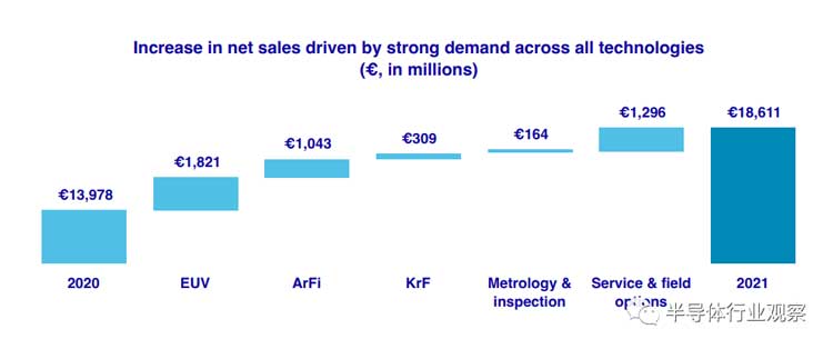
Sales of DUV systems also increased from 227 in 2020 to 267 in 2021. In addition to EUV and DUV sale growth, service and field option sales were also the drivers of ASML's overall net sales growth. This growth was driven by productivity, coverage, and upgrade kit sales growth. The DUV systems provide the most efficient way to rapidly ramp up wafer production, which is supported by a growing installed base.
To meet customer demand for additional wafer capacity, ASML has accelerated delivery of capacity upgrades, even before Factory Acceptance Testing (FAT) completion, expediting system delivery.
It is not difficult to see that the digital transformation and the current shortage of chips have further contributed to ASML's need to increase its production capacity. On the one hand, logic demand for advanced and mature nodes continues to be strong, driven by digital transformation and distributed computing. On the other hand, memory demand continues to grow due to market demand for servers and smartphone terminals. In order to meet the demand growth for DRAM and NAND, customers should improve production capacity and migrate nodes. ASML expects EUV memory requirements to continuously increase as the customers are mitigating to more advanced nodes.

The incomes of ASML from the logic, memory, and service markets from 2019 to 2021 (unit: million euros).
In terms of R&D investments, ASML's R&D costs in 2021 are EUR 2.547 billion. Compared to the investment of EUR 2.208 billion in 2020, these increased investments relate to total lithography solutions for EUV, DUV, and application projects, the most important of which is the continued strengthening of mass production of EUV and the development of EUV0.55NA.
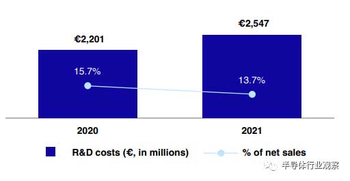
ASML's R&D investment from 2020 to 2021 (unit: million euros)
ASML expects net sales to increase by approximately 20% in 2022 compared to 2021 due to healthy logic demand and growth in the memory market. The expected growth is driven by higher sales across platforms and growth in the base install business.
Logic chip segment: The expanding application space and long-term growth momentum have translated into strong demand for advanced and mature nodes. Logic systems revenue is expected to grow by more than 20% year over year as demand continues to be high.
Memory: Supports expected growth as system utilization improves and customer technology transitions. Additional production capacity is expected to be required. Therefore, the demand for lithography equipment in the memory market in 2022 will be strong, and the year-on-year growth of system revenue will increase by about 25%
EUV Equipment: Approximately 55 EUV systems are expected to ship in 2022 as customer usage and confidence in EUV increases. Six out of 55 system revenue recognition will be deferred to 2023. EUV system revenue is considered to increase by 25% % in 2022.
Non-EUV Systems: In the DUV and Applications business, ASML forecasts an increase in immersion and dry systems, and demand for measurement and inspection systems will continue to increase. Non-EUV transportation revenue is expected to increase by more than 20%.
Looking ahead to 2025 to 2030, this decade will revolve around distributed computing, bringing the cloud closer to edge devices. Through connectivity, computing power will connect the world by providing everyone with device computing power. The general trends in the global electronics industry are expected to continue to drive the growth of the overall semiconductor market, which is supported by a highly profitable and innovative ecosystem.
This means that the demand for wafers at advanced and mature nodes is increasing, thereby increasing the demand for lithography equipment. ASML believes that annual sales can reach 24 billion-30 billion euros in 2025, with gross profit margins between 54% and 56%.
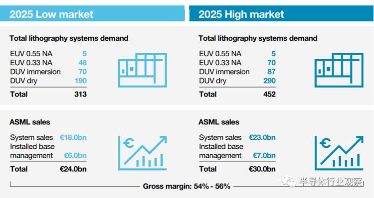
ASML's market forecast (source: ASML)
 Infringement event
The ASML annual report mentions that ASML may be subject to malicious attacks, including stealing trade secrets, proprietary customer data, intellectual property, and other confidential information by third parties or our own employees. Although ASML attempts to protect intellectual property rights, know-how, products, designs, technologies, and other intellectual property rights may be obtained, copied, used, or disclosed by unauthorized third parties. In 2021, ASML learned that DJEL, which is related to XTAL, is actively marketing products that may infringe ASML's intellectual property rights.
Recently, DJEL issued a statement saying that since its establishment, OJEL has been abiding by Chinese laws and operating in compliance with the laws and regulations. DJEL adheres to the concept of independent research, development, and innovation. It respects and protects intellectual property rights and forms an independent and perfect intellectual property system. Although DJEL's statement did not mention ASML, it clearly meant a response and a rebuttal.
According to public information, XTAL was founded in 2014 by former ASML employees. In 2016, ASML sued XTAL. In 2018, a federal court in Santa Clara, California, initially found XTAL guilty of intellectual property theft. In 2019, the court issued a final judgment, and finally, ASML won.
In 2019, the Dutch financial newspaper reported that Chinese employees stole company secrets from ASML and caused hundreds of millions of dollars in losses. According to reports, senior Chinese employees in the research and development department of ASML's US subsidiary stole the technology, which was eventually leaked to the Chinese company.
However, ASML might not want to expand the event. In 2019, ASML issued an official statement on its official website to clarify that ASML disagrees with Chinese spy activity.
In 2021, DJEL completed the excellent verification of the yield rate of silicon wafers for key process layers of 28nm logic chips and continuously broke through technical barriers. The 14nm computational lithography technology was all set, and the first set of EBI industrialization has achieved remarkable results. In 2021, the company achieved the small goal of rapid sales growth of more than 100 million yuan and contacted nearly 60 customers.
However, because of relatively-low product performance, DJEL's products cannot threaten the leading position of ASML. However, ASML mentioned that DJEL might have a relationship with XTAL, which was awarded compensation for stealing secrets in 2018. ASML reminded its specific customers not to assist or condone DJEL in potential infringement and expressed concern about Chinese authorities.
ASML said it was monitoring the issue closely and was prepared to take legal action, but it did not provide further evidence. This statement rarely appears in financial reports, leading to Inevitably consideration.
Source: Semiconductor Industrial Perspective, retrieved by Fitech




 Back to list


