The Application of Solder to Produce Micro-Bumps in SiP
With the development of the package size in semiconductor packaging to below ten nanometers, Moore's Law has reached its limit. Manufacturers developed a technology to realize semiconductor chip integration with a smaller chip size. The application of SiP is to integrate multiple microchips under Moore's Law limit conditions through multi-material and multi-dimensional space integration, thereby expanding the function of the chip and making an integrated chip combination to achieve the sensor and control chip packaging of 5G, IoT, etc. Once the chips are integrated and packaged, it is necessary to use BGA packaging to connect the electrical signals of each chip to the substrate PCB, COB, FPC, etc. Since these connection point sizes are below 100μm, the original 0.1mm and 0.2mm BGA balls can no longer meet the micro-connection requirements. The manufacture of microspheres below 100μm, such as 0.08, 0.07mm, is limited by the process, resulting in high price and low production capacity. Besides, the ball machine suitable for 0.08mm micro balls is expensive and difficult to operate. These are a bottleneck in the process development of SiP integrated packaging.
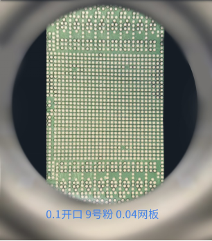
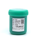
As shown in the figure below, Fitech’s T8 (2-7μm) and T9 (1-5μm) ultra-fine solder pastes can produce micro solder joints on pads( <100μm).

The packaging step of solder paste printing, reflow soldering under nitrogen protection, water-based cleaning, and height adjustment can replace the original BGA process to realize SiP. This method improves the process efficiency and avoids using complicated and expensive ball-attach machines and ball-attach processes. It provides an economical and feasible material and process solution for SiP.


 Back to list


