Reliability assessment of ultra-thin 3D-IC packages under the influence of coupled loads from manufacturing process and temperature cycling tests-Shenzhen Fitech

Reliability assessment of ultra-thin 3D-IC packages under the influence of coupled loads from manufacturing processes and temperature cycling tests
In response to the Internet of Things and smart manufacturing, the design of semiconductor chip structures based on Moore's Law involves a reduction in the size of the associated electronic components. As a result, the density of transistors gradually increases. To achieve the above packaging requirements and to solve the bottleneck of the traditional packaging framework, existing research is dominated by three-dimensional interconnects in the stacking direction. The key technologies are silicon through-hole (TSV) and solder micro-bump (μbump) interconnects, which are usually the area of concern in terms of failure location. Three-dimensional integrated circuit (3D-IC) packages have many manufacturing process and reliability challenges to overcome, with accelerated thermal cycling testing (TCT) reliability issues being particularly critical. According to the JESD22-A104D specification, a severe coefficient of thermal expansion (CTE) mismatch between package components can produce significant thermal stress on the critical solder μbump under thermal load.
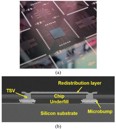
Figure 1. actual ultra-thin chip 3D-IC package
Garofalo-Arrhenius creep model
When a material is subjected to a fixed load at a temperature of 0.5 T m above its melting point, the strain increases with time. This phenomenon is called creep. Figure 2 shows that the creep behavior of ductile materials under fixed stress and temperature can be divided into three phases, namely primary, secondary and tertiary creep. The steady-state region accounts for most of the creep deformation. For solder joints applied in electronic packaging, the Garofalo-Arrhenius model, also known as the hyperbolic sine model, is widely used to define the creep behavior. The second stage, shown in Figure 2, exhibits steady-state creep and is described by the Garofalo-Arrhenius model.
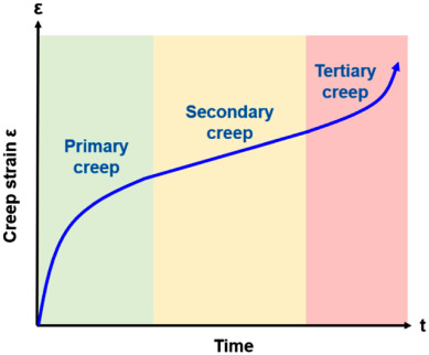
Figure 2. Creep strain versus time for solder alloys under fixed stress.
Table 1 lists the detailed material properties used in this FEA. In order to accurately predict the creep behavior and package warpage of SnAg μbump, we assigned nonlinear material properties to solder and copper [ 34 ]. The solder exhibited temperature-dependent properties and creep behavior. The coefficients of the Garofalo-Arrhenius creep model for SnAg solder are presented in Table 2. As the maximum temperature of the thermal cyclic load (125°C) exceeds the glass transition temperature (Tg) of the molded material (110°C), the Young's modulus of the molded material is greatly reduced, which affects the mechanical properties of the molded material throughout the package. Therefore, Tg should be considered as the molding material in the current FEA.
Table 1. List of material properties currently used in 3D-IC packaging FEA.
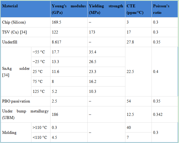
Table 2. Parameters of Garofalo-Arrhenius model for 96.5Sn3.5Ag solder [ 32 ].

Due to the large temperature variations during the associated assembly process, residual stresses are often induced within the packaging structure that have a considerable impact on reliability. In this study, the actual mechanical state of the packaging device prior to TCT is predicted by elucidating the problems and effects of the proposed coupling loads. The ultrathin chip fabrication process for 3D-IC packages involves coarse grinding of copper-filled TSV chips to 100 μm and adjusting their connection to the silicon substrate. Under hot pressing at 250 °C, the chip and substrate are bonded together to form a 15 μm gap, which is then filled with bottom-fill material by capillary action. Thereafter, a thicker molding material is applied to the chip to disperse the grinding load on the chip, thus avoiding chip breakage when the 100 μm thick chip is further ground down to 10 μm thickness. The passivation layer is then deposited on the top surface of the assembled chip. The creep behavior of μbumps is neglected in the simulation of the fabrication process due to the time limit relative to the TCT duration. The TCT conditions used in this paper follow the JEDEC standard JESD22-A104 condition D. The temperature range is between -40 °C and 125 °C. Heating from room temperature at 25 °C to 125 °C takes 450 seconds. The 125 °C temperature is then held for 900 seconds. The temperature then drops from 125 °C to -40 °C in 900 s. Finally, the temperature returns to 25 °C in 450 s. A TCT lasts 3600 s. In this work, seven complete TCTs were performed in FEA to obtain convergence, incremental and equivalent plastic and creep strains for the critical solder μ-bump.
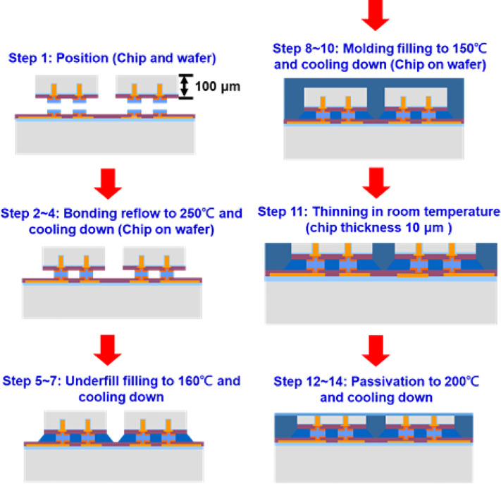
Figure 5. Schematic diagram of the proposed manufacturing process for ultra-thin chips in 3D-IC package.
Figure 6 shows the incremental and equivalent plastic and creep strains affected by the coupled loading of the manufacturing process and TCT. The peak strains occur later in the process when the temperature returns to room temperature, as this is when the most significant CTE mismatch is introduced in the package assembly. Take for example the case of step 12, where the structural stiffness is reduced by chip thinning. When the package is heated to 200 °C, significant incremental plastic strain peaks and equivalent plastic strain peaks are estimated. Furthermore, the analysis shows that the incremental and equivalent creep strains of μbumps are almost the same as their incremental and equivalent plastic strains after seven TCTs. Therefore, the creep effect of the SnAg solder μbumps cannot be ignored when assessing the reliability of TCT. Figure 7 shows the warpage variation of the entire package structure at each fabrication step and in TCT. The severe warpage in step 12 can be attributed to an increase in critical deformation that causes a corresponding incremental and equivalent plastic strain. In addition, the warpage variation caused by the TCT relative to the fabrication part is rather small. In other words, the effect of residual stresses in the manufacturing process needs to be considered in the subsequent reliability assessment of the TCT.

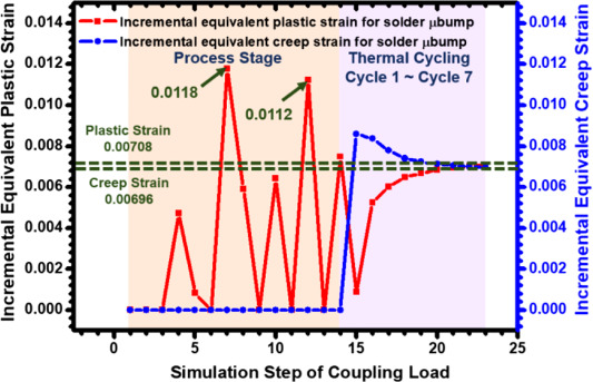
Fig. 6. Variation of the estimated equivalent plasticity and creep strain increments for the outermost solder μbumps under coupling load of TCT.

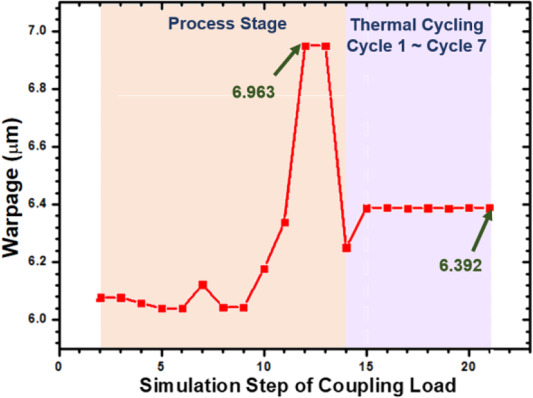
Fig. 7. Predicted warpage variation of the ultra-thin chip in 3D-IC package under the processing step and subsequent TCT based on the proposed simulation method.
5.1.Assembled chip thickness
as shown in Figure 8. As the chip thickness increases to greater than ~20 μm, the strain increment increases. This phenomenon becomes widespread with the use of bottom-fill materials with high Young's modulus. At the chip thickness transition between 20 and 50 μm, the chip shows the least structural resilience. Therefore, the main mechanism affecting the reliability of μbump is the CTE mismatch between the bottom filler material and the PBO material. However, with the adoption of a rigid thickness layer, the thermal mismatch between the TSV of the filled copper and the chip increases. As a result, μbumps accumulate and sustain larger shear strains during fabrication and under the load of TCT. This situation leads to an increase in inelastic strain. In contrast, when the bottom filler with low Young's modulus is used as a stress buffer layer to disperse the shear deformation of μbump, the strain increment of μbump can be reduced.


Figure 8. Dependence of the chip thickness on the equivalent inelastic strain increment on the critical μbump when considering bottom fills with different Young's modulus values.
5.2.TSV spacing effect
As shown in Figure 9 the equivalent inelastic strain increment decreases slightly when the TSV spacing is extended from 170 μm to 250 μm. The reason can be attributed to the fact that the strain caused by the CTE mismatch between the different materials can be uniformly distributed to each solder μbump. however, with the application of various bottom fillers, significant differences in the strain magnitude are observed. The results indicate that the strain increment for μbump with lower bottom filler Young's modulus decreases while maintaining the same pitch. Thus, the designed parameter, i.e., the bottom-filled Young's modulus, is more sensitive than the TSV spacing in reducing the μbump strain. The results of the analysis indicate that a bottom fill with a Young's modulus of 0.3 GPa is a good choice for reducing the accumulation of critical μbump strain.

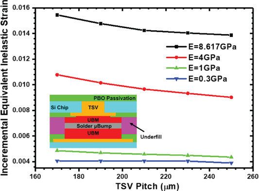
Figure 9. Dependence of TSV spacing on μbump inelastic strain increments when four different Young's moduli of the bottom-filled adhesive are considered.
5.3.TSV radius effect
For the parametric analysis of the TSV radius, the estimated results are shown in Figure 10. Similar to the previous discussion on other parameters, the low Young's modulus of the bottom-filled adhesive results in a lower strain increment for μbump when the radius size of the TSV is fixed. An increase in the radius of the TSV usually leads to a larger strain increment. Nevertheless, assembled chips with a 25 μm TSV radius and bottom-fill with Young's modulus of 4 and 8.617 GPa reduce the μbump strain. Therefore, the estimation results indicate that the TSV radius is related to the strain increment of μbump. As the TSV radius is expanded from 10 μm to 25 μm, the contact area with the PBO material is also expanded. Severe deformation due to CTE mismatch between package components can increase the μbump strain. In addition to the under-bump metallurgical layer (UBM), the underfill that also encases the solder μbump has a low Young's modulus, which improves the flexibility of the structure. As a result, the above strains can be significantly reduced. When the TSV radius is 25 μm, the UBM layer attached to the top of the solder μbump has the same diameter and the strain inside the μbump increases. The use of a bottom filler adhesive with a Young's modulus of 4.0 or 8.617 GPa is effective in resisting the μbump strain. Therefore, the decrease of the μbump strain increment was investigated. Contrary to the observations for bottom fillers with Young's modulus of 0.3 or 1, bottom fillers with Young's modulus of 4.0 or 8.617 GPa have very limited ability to suppress package warpage, although the μbump strain can still be released at this point. As a result, the final strain is slightly increased.
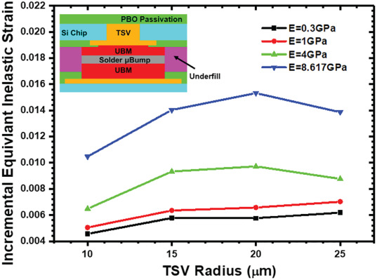
Figure 10. Dependence of TSV radius on μbump inelastic strain increments when considering several Young's moduli for bottom filling.
Conclusion
The analysis shows that the package structure undergoes severe warpage during the processing stage due to the drastic change in temperature relative to the TCT temperature. The convergent warpage is almost reached before TCT. In addition, plastic strain accumulates heavily within the solder μbump during the manufacturing process. This situation leads to a reduction of plastic accumulation during TCT. Nevertheless, the creep behavior should be considered, since the creep strain in the μbump reaches half of its own inelastic strain accumulation through the TCT loading.
Regarding the parametric analysis, the estimation results show that a relatively thin chip can obtain a good structural flexibility to release the strain of the solder μbump. The longer TSV spacing also facilitates the dispersion of the CTE mismatch deformation transferred to the μbump, resulting in a low strain increment. As for the TSV radius, a larger radius was found to result in an increased contact area between the copper-filled TSV and the PBO layer. Therefore, the strain increase in the critical μbump is mainly due to the severe CTE deformation of the package material. In addition, selecting a bottom filler material with low Young's modulus, which is considered as a stress buffering mechanism, is a good way to meet the reliability requirements of solder μbumps.
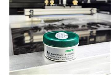
After 20 years of solder paste R&D and application experience, Shenzhen Fitech can manufacture ultra-fine solder paste products (T6 and above) with excellent wettability, tackiness, viscosity stability, low void ratio, and high mechanical strength, which can meet the requirements of the large-scale production of ultra-fine-pitch electronic components. Please let us know if you need more information.

References
Chang-Chun Lee, Yu-Min Lin, Hou-Chun Liu, Ji-Yuan Syu, Yuan-Cheng Huang & Tao-Chih Chang(2021). Reliability evaluation of ultra thin 3D-IC package under the coupling load effects of the manufacturing process and temperature cycling test. Microelectronic Engineering, vol. 244-266.





 Back to list


