Influences of Transfer Efficiency and Reflow Profile on Printing Solder Paste
Influences of Transfer Efficiency and Reflow Profile on Printing Solder Paste
As miniaturization continues and usage requirements become higher, the number of pads on the chip is also increasing. In order to meet the massive solder joint packaging, manufacturers prefer to use the printing process. The solder paste printing process is efficient and can complete large-area printing in a short time, which can be used for large-scale chip packaging. Solder paste is uniformly placed on the stencil, and a squeegee is used to fill the solder paste in the stencil openings. After the solder joints are printed, it needs to melt and solidify into solder joints through a reflow soldering process.
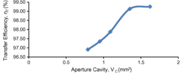
Transfer efficiency is related to the stencil opening and squeegee's speed. Due to the shear force, the speed of the squeegee affects the viscosity change and the transfer efficiency of solder paste through the apertures. In addition, the size of the opening affects the amount of solder paste that deposits on the pads. The relationship between aperture size and transfer efficiency is shown in Figure.1. This remarkable printing behavior of solder paste may be caused by surface tension, the cohesion of solder constituent particles, and adhesion forces that exist between the solder and the aperture walls (Amula et al., 2011).

Figure 1. Transfer efficiency vs. aperture cavity (Amula et al., 2011).
During the reflow soldering process, a reflow oven is used to heat the assembled PCBs to a preset temperature at an appropriate heating rate for a specified period of time. This process requires the use of a thermal curve time-temperature plot to adjust the temperature change parameters. The reflow process includes preheating, soak, reflow, and cooling zones, which is an important factor affecting the microstructure and reliability of solder joints. The soldering process requires a peak reflow temperature above the melting point of the solder and a reflow time long enough to maximize solder paste wetting of the pads, which allows chemical and metallurgical reactions to complete in the solder. For example, the melting point of SAC305 solder paste is 217°C, and the peak reflow temperature needs to be higher than the melting point to melt and wet the pad. Higher cooling rates can reduce the grain size and the intermetallic growth rate. Generally, the cooling rate should be controlled at 4°C/s.
For the tin-bismuth paste, a short time above liquidus (TAL) and a low peak temperature can minimize the formation of the IMC layer between the solder and the PCBs, while it can lead to poor soldering. Conversely, long TAL and high peak temperature favor interfacial reactions, but excessive Bi segregation can make solder joints brittle. Table 1 confirms that higher peak temperature and longer TAL are beneficial for solder paste wetting coverage. However, excessively high temperature weakens the wetting ability. Longer TAL allows more time for oxide volatilization, which facilitates wetting.
Table 1. Reflow profile impacts on the SnBi solder paste wetting performance (Amula et al., 2011).
In brief, transfer efficiency affects printing efficiency and affects solder paste volume. The reflow profile affects the solder wetting ability and solder joint quality.
Reference
Amula, E.H., Lau, W.K., Ekere, N.N., Bhatti, R.S., Mallik, S., Otiaba, K.C., & Takyi, G. (2011), “A study of SnAgCu solder paste transfer efficiency and effects of optimal reflow profile on solder deposits”, Microelectronic Engineering, vol.88(7), pp.1610-1617.
Dusek, K., Busek, D., Vesely, P., Prazanova, A., Placek, M., & Del Re, J. (2022), “Understanding the Effect of Reflow Profile on the Metallurgical Properties of Tin–Bismuth Solders”.


 Back to list


