Electromigration Influences of Lead-Free Solder Paste on Solder Joint Reliability
Electromigration Influences of Lead-Free Solder Paste on Solder Joint Reliability
With the increasing demand and miniaturization of electronic devices, electromigration poses a challenge not only to the reliability of integrated circuits, but also to the reliability of electronic packaging. Electromigration is one of the factors that affects the reliability of solder joints. When the electronic equipment is operated, current stress will be generated to form a certain current density at the solder joints. As the number of I/Os increases, the current density also increases. The current density is the driving force for the atom migration and the growth of intermetallic compounds (IMC). Continuous current stress can lead to open circuit issues over time.
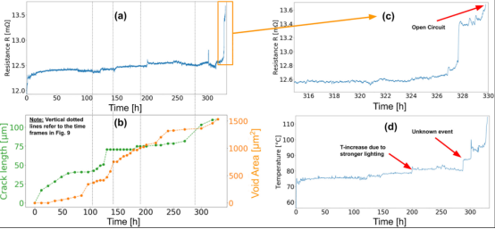
Electromigration is the diffusion of metal ions caused by the momentum transfer of mobile electrons. Electromigration occurs when an anode and a cathode are present in the element. Under current stress, the directional atomic transport in the interconnected solder joints accelerates the UBM depletion and asymmetric growth of the IMC layers, and leads to defects such as voids and cracks. Lead-free solder pastes are prone to electromigration due to the lower melting point of lead-free solder pastes resulting in higher diffusivity. Rapid electromigration can lead to solder joint failure. AbdelAziz et al. (2021) tested the change in the resistance of SAC305 solder joints and found that the resistivity increased significantly at more than 300 hours, indicating the occurrence of electromigration (Figure 1). Besides, solder joint cracks and voids change over time.

Figure 1. SAC305 solder joint electrical resistance changes, I=5A (AbdelAziz et al., 2021).

Figure 2. Profile of a SAC305 solder joint in different time, (a) 0, (b) 102, (c) 139, (d) 171 and (e) 276 h, (AbdelAziz et al., 2021).
As can be seen from Figure 2, cracks appeared in the top and bottom left corners of the SAC305 solder joints, and voids (black areas) appeared above the solder joints.
Similarly, Zuo et al. (2015) conducted electromigration tests on eutectic SnBi solder paste and found that in the late testing stage of the coupling effect of electrical and thermal stress, high current density caused electromigration, which changed the interfacial mechanics caused by mass transport. It accelerated the IMC formation and eventually led to solder joint failure. The experimental results of Zuo et al. showed that visible voids and rod-like bismuth extrusions appeared in the solder joints after 260 hours of electrothermal coupled stress (Fig. 3). The crack developed and the Cu-Sn IMC thickness became larger, showing a positive correlation with time.

Figure 3. The SEM images of SnBi58 solder paste after 260 hours with current density of 2x10³A/cm2 (a) canode,(b) anode (Zuo et al., 2015)
Fitech is committed to producing high-reliability ultra-fine solder paste products. Fitech and can adjust solder paste parameters according to customer requirements. Welcome to consult and learn more.
Reference
AbdelAziz, M., Xu, D.E., Wang, G.T., & Mayer, M. (2021), “Electromigration in solder joints: A cross-sectioned model system for real-time observation”, Microelectronics Reliability, vol.119.
Zuo, Y., Ma, L.M., Liu, S.H., Shu, Y.T., & Guo, F. (2013), “Evolution of Microstructure Across Eutectic Sn-Bi Solder Joints Under Simultaneous Thermal Cycling and Current Stressing”, Journal of Electronic Materials, vol.44.


 Back to list


