Solder Paste Micro-Bump Geometric Shape
Solder Paste Micro-Bump Geometric Shape
With the development of packaging technology, to meet higher packaging requirements, an increasing number of manufacturers have begun to adopt BGA technology. By printing solder paste on the pads. The BGA process can form micro-bumps after reflow. The components can be soldered to the bumps later on. The process of solder paste printing needs to be precisely controlled because the bump geometry has an impact on the solder joint reliability. Surface tension, the contact angle between solder paste and pad, and density are the key factors affecting the material characteristics of solder bump geometric shape. Therefore, a better understanding of the geometry of solder bumps is required to address microarchitectural design in semiconductor technology.
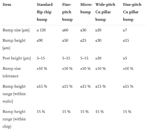
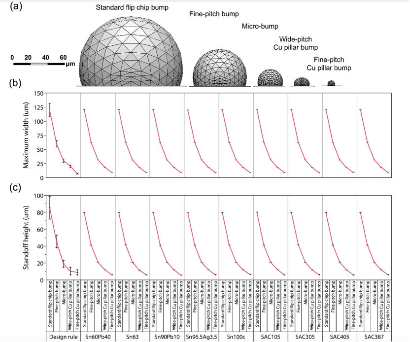
Bump structures can be used to address package requirements of various sizes. The surface tension of the solder paste bumps, solder pad contact angle, and density determine the minimum achievable bump surface area. Yusof et al. (2022) used different types of solder pastes for bump fabrication and observed the geometry (Figure 1). It can be seen from Figure 2 that regarding mainstream bump technology, the standard flip-chip bump has the largest size, while the fine-pitch copper pillar bump is the smallest.

Figure 1. Solder density and surface tension (Yusof et al., 2022).

Figure 2. Different standards of bumps (Yusof et al., 2022).
According to the simulation results of Yusof et al., the percentage difference between the average maximum width and the average height of solder paste bumps with the structure predicted by Surface Evolver software increases as the solder paste volume decreases. The resulting difference between the maximum width and height is the largest due to the smallest size of the fine-pitch Cu pillar bumps. Furthermore, since the total energy required to achieve static equilibrium forces increases with dropping volume, it is difficult to achieve stability with smaller bump sizes. From standard flip chips to the smallest fine pitch copper pillars, the total energy reduction per initial area required to reach equilibrium increases hundreds of times.

Figure 3. Geometric sizes of bumps produced by different solder pastes simulated by Surface Evolver (Yusof et al., 2022).
Greater surface tension causes a larger contact angle between the solder paste and the pad. Therefore, the height of the bump will increase. And high tension will reduce wide surface area and width. Density changes also affect height, and increased density will result in smaller bump heights. The combined impacts of gravity, high density, and high tension in the reflow process reduce the height and width of the bumps.
Fitech specializes in the production of solder paste products that can be used in bump technology. The bumps are round, and the ratio of width and height after soldering is outstanding. Welcome to consult and understand.
Reference
Ab Aziz bin Mohd Yusof, Mohd Al Fatihhi Mohd Szali Januddi, & Muhamad Noor Harun. (2022), “A study of micro-scale solder bump geometric shapes using minimizing energy approach for different solder materials, Ain Shams Engineering Journal”, vol.13(6).


 Back to list


