Lead-Free Solder Paste_ Effects of PCB Nickel Plating on Soldering

https://en.szfitech.com/
Lead-Free Solder Paste_ Effects of PCB Nickel Plating on Soldering
The development trend of microelectronics requires high-performance and high-density electronic components. However, intermetallic compounds (IMCs) will affect the reliability of high-density electronic components. The surface finishes of PCBs have a noticeable influence on the formation of IMCs. Currently, the market has studied several surface finish methods of PCBs to improve the soldering effect, including organic flux (OSP), ENIG, ENEPIG, etc. ENIG and ENEPIG surface-finished PCBs are widely used. For ENIG and ENEPIG, different nickel layer thicknesses will affect the soldering effect. This article briefly introduces the influence of the nickel layer on soldering.
Effects of Nickel Layers on the Solderability of PCBs
It is generally found in the industry that there is a risk of the black pad in the ENIG process. The reason for the occurrence of the black pad is that the nickel atom is smaller than the gold atom, and the grains are rough after gold plating due to the different atomic sizes. The gold plating solution will penetrate into the nickel layer and corrode it, resulting in the generation of poor-solderability nickel oxide. Due to the oxidation of nickel layers, it is difficult to form a metallurgical bonding for the solder pastes and copper pad, and the solder joints are easy to strip.
In order to solve the black pad problem, the industry has introduced the ENEPIG surface finish technology. The nickel layer is plated with palladium, which effectively avoids the corrosion of the nickel layer. In addition to the black pad problem, the nickel layer also affects the growth of IMCs. The nickel layer thickness of ENEPIG needs to be further optimized. In order to study the influence of ENEPIG nickel layer thickness, Kim et al. used SAC305 solder paste to conduct soldering on ENEPIG-treated PCBs. ENEPIG-treated PCBs with different nickel layer thicknesses were used for analysis.

Figure 1. Schematic diagram of SAC305 solder paste on the ENEPIG circuit board. (a) Nickel layer 4-6 μm; (b) Nickel layer 0.3-1 μm.
Effect of Nickel Layer Thickness on IMCs
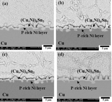
It can be seen from Figure 2 that (Cu, Ni) 6Sn5 is formed in all nickel layer thicknesses. During soldering, Au and Pd on the nickel layers will melt into SAC305 solder paste, and then Sn and Cu in the solder will diffuse to the nickel layer and react to form (Cu, Ni) 6Sn5. In addition, when the nickel layer is thin, the growth rate of (Cu, Ni) 6Sn5 is faster.

Figure 2. Soldering effect of SAC305 solder paste on a ENEPIG circuit board. (a) Nickel layer 0.3 μm; (b) Nickel layer 0.5 μ m; (c) Nickel layer 0.7 μ m; (d) Nickel layer 1 μm.
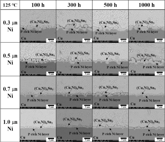
After aging for 1000 hours, the thickness of the (Cu, Ni) 6Sn5 layer of the sample with a 3μm nickel layer reached the largest, which is much greater than that of the sample with a 1μm nickel layer. What’s more, if the thickness of the nickel layer is extremely small, (Cu, Ni) 6Sn5 will significantly expand to the bottom of the interface. When the nickel layer thickness increases to 0.7μm and above, (Cu, Ni) 6Sn5 at the bottom of the interface becomes less. This is because the P-rich nickel layer acts as a barrier to the diffusion of Sn and Cu during aging, slowing down the growth of IMCs. In addition, the smaller the nickel layer thickness, the greater the total thickness of IMC generated.

Figure 3. SAC305 solder joints aged at 125 ℃ for 1000 hours with different PCB's Ni layer thickness.
Effect of Nickel Layer on Mechanical Strength of Solder Joints
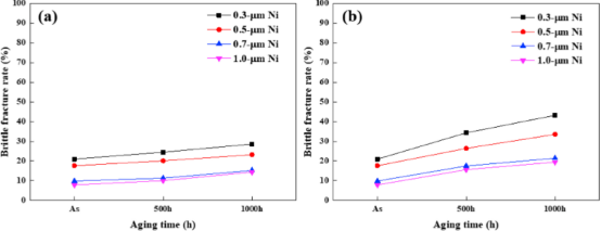
When the thickness of the nickel layer is 0.3μm, the mechanical strength of solder joints after aging is the worst, and the failure probability of the solder joint is far greater than that of the experimental samples with a nickel layer thickness of 0.7μm and 1μm. The thinner nickel layer will bring more IMCs, and the enrichment of IMCs will increase the brittleness of solder joints. As a result, brittle fracture is easy to occur after aging. At the same time, brittle fracture is related to aging temperature. For solder joints with smaller nickel layer thickness, IMC growth is more sensitive to high temperatures, and the brittle fracture rate increases faster.

Figure 4. Relationship between Ni layer thickness and solder joint strength. (a) Aging at 125 ℃; (b) Aging at 150 ℃.
Shenzhen Fitech can produce solder paste products suitable for ENIG and ENEPIG-treated PCBs. Fitech’s solder paste products have excellent wettability, mechanical strength, and thermal and electrical conductivity after soldering. Welcome to contact us.
Reference
Kim, J., Jung, S.B. & Yoon, J.W. (2019). “Optimal Ni(P) thickness and reliability evaluation of thin-Au/Pd(P)/Ni(P) surface-finish with Sn-3.0Ag-0.5Cu solder joints”. Journal of Alloys and Compounds, vol.805, pp.1013-1024.


 Back to list


