Solder Paste Introduction: Influence of Solder Layer Thickness on Cu3Sn Phase
Solder Paste Introduction: Influence of Solder Layer Thickness on Cu3Sn Phase
With the evolution of microelectronic packaging technology and the increases in the user’s needs, advanced integration technologies such as 3D packaging and wafer-level packaging have been developed. Cu-Cu and Cu-Sn-Cu are the most common interconnections in packaging. As a soldering material, lead-free solder paste can react with copper metallurgically, thus connecting copper bumps and copper pads. However, the growth of intermetallic compounds (IMCs) in a lead-free soldering system is challenging to avoid. The development of IMCs will affect the mechanical and thermoelectric properties of the miniaturized package. In order to optimize the IMC thickness after soldering, A large number of researchers have analyzed the influence of solder layer thickness on the Cu3Sn phase.

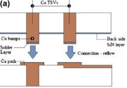
Figure 1. Cu-Sn-Cu interconnection schematic diagram.
In the soldering process, the molten lead-free solder paste will react with Cu, making Cu6Sn5 nucleate at the Cu–Sn interface. Cu atoms continue to dissolve until the solder paste at the interface becomes supersaturated. Cu6Sn5 microcrystals can nucleate and grow rapidly. The diffusion of Sn and Cu is the main reason for the formation of Cu6Sn5. The development of Cu3Sn frequently occurs in the aging process.
Growth Mechanism of Cu3Sn Phase
Compared with the as-reflow condition, thermal aging will significantly increase the total thickness of IMCs. During aging, Sn will continue to diffuse to provide the driving force for IMC growth. Therefore, the total thickness increases continuously during aging, while the Sn layer will eventually run out. After Sn depletion, Cu6Sn5 will be gradually consumed and form Cu3Sn, resulting in the decrease of Cu6Sn5 thickness.

Effect of Solder Layer Thickness on Cu3Sn
In the conventional soldering process, the thickness of the solder layer is about 20 μm. When the thickness of the solder layer is large, the Sn flows smoothly, the growth rate of Cu6Sn5 is fast, and the appearance of the Cu3Sn phase is restrained. Longer aging time is required to realize the depletion of Sn, and then Cu3Sn starts to grow slowly. Li and Chan tried to reduce the thickness of the lead-free solder paste layer to the sub-micrometer level to verify the influence of solder layer thickness on IMC growth.

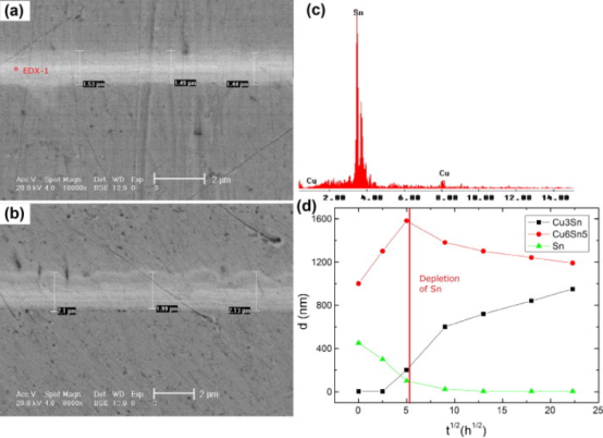
Figure 2. The growth of IMC layers with solder layer thickness of 1μm. (a) As-reflowed; (b) Aging for 100h; (c) EDX results; (d) IMC change trend.
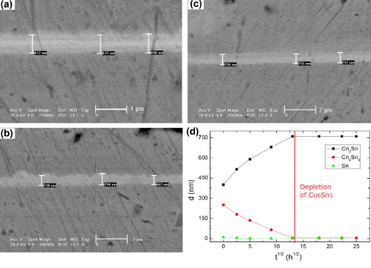
Figure 2. The growth of IMC layers with solder layer thickness of 500nm. (a) As-reflowed; (b) Aging for 100h; (c) Aging for 500h; (d) IMC change trend.
Figure 2 shows that the solder layer was delaminated, representing Cu6Sn5 and Cu3Sn layers appeared. After thermal aging, the Sn layer continued to provide Sn atoms for the IMC layers and promoted the growth of IMC. It can be seen from Figure 3 that Cu6Sn5 and Cu3Sn layers were observed when the solder layer thickness was 500nm, but the boundary was not obvious. As the amount of Sn was insufficient, it was exhausted during reflow soldering. It is widely confirmed that the nucleation and growth of Cu3Sn are realized by consuming Cu6Sn5Sn. In addition, it can be known that the thin solder layer will cause fewer IMCs, and the Cu6Sn5 thickness is insufficient. Thus, the conversion of Cu6Sn5 to Cu3Sn will be limited.
Fitech can produce ultra-fine solder pastes for ultra-fine-pitch soldering, with excellent wettability and high solder joint reliability. Welcome to the official website for more information.
Reference
Li, Q. & Chan, T.C. (2013). “Growth kinetics of the Cu3Sn phase and void formation of sub-micrometre solder layers in Sn–Cu binary and Cu–Sn–Cu sandwich structures”. Journal of Alloys and Compounds, vol.567, pp.47-53.


 Back to list


