Medium-Temperature Solder Application_ Reflow Process Optimization for Fan-out Packaging

https://en.szfitech.com/
Medium-Temperature Solder Application_ Reflow Process Optimization for Fan-out Packaging
Fan-out wafer level packaging (FOWFLP) allows more I/O terminals outside the chip surface, which brings more advantages than fan-in packaging. The development of fan-out packaging breaks through the limitation of I/O terminals in equipment and is considered a packaging solution in the post-Moore era. Fan-out packaging usually involves dicing chips on a silicon wafer, placing known-good chips precisely on thin reconstituted or carrier wafers, and then molding them. After that, a redistribution layer (RDL) is formed at the top of the molding area (chip and fan-out area and solder balls are placed.
SAC305 lead-free solder joint test
The lead-free solder balls can be made with medium-temperature solders, such as SAC305, which are transferred to the pads through the BGA process. This article mainly analyzes the reliability of the fan-out packaging of SAC305 BGA solder joints. The optimization of the reflow process is also included. Reliability can be confirmed by solder joint structure and shear strength. Zhang et al. designed a PCB for a specific fan-out package. By controlling different reflow times and peak temperatures, they tested the reliability of a fan-out-package device (72 solder joints) and studied the microstructure, shear strength, and failure mode of solder joints.

Figure 1. Experimental Fan-out Packaging Device (Zhang et al., 2022).
Test results of different reflow processes
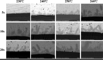
Zhang et al. found that the SAC305 solder ball was metallurgically connected with the ENIG electrode to form intermetallic compounds (IMCs) after reflowing at the peak temperature of 230°C for 5s. IMCs began to appear at 5 seconds during reflow. At this stage, (Cu, Ni) 6Sn5 was the major IMC, but the IMC thickness was thin, and the metallurgical bonding strength of the solder joint was still weak. (Cu, Ni) 6Sn5 grew with time, and the grain gradually coarsened. In addition, when the peak reflow temperature climbed to 260°C and reflow time increased to 10s, (Cu, Ni) 6Sn5 grains grew moderately at the Sn-ENIG interface. The grain shape of (Cu, Ni) 6Sn5 is mainly bar-shaped and uniformly distributed. As the reflow time increases, a large increase in the thickness of brittle (Cu, Ni) 6Sn5 will lead to a decrease in mechanical properties, increasing the fracture probability of solder joints.

Figure. 2. Effects of peak reflow temperatures and time on solder joint microstructure (Zhang et al., 2022).
When the peak temperature was set at 260℃ and the reflow time increased to 20s, the Sn atoms diffused to the surface of the nickel-plating pad and gradually flew under the pad. The Sn atoms reacted with the Cu atoms and converted into (Cu, Ni) 6Sn5, which led to the pad volume shrinkage and the pad peeled off from the PCB. What’s more, if the PCB is under high temperature, excessively long reflow time makes solder atoms diffuse to the PCB surface, which increases the stress on the PCB surface. As a result, the pad is likely to peel off during use, causing poor solder joint reliability (Zhang et al., 2022).

Figure 3. IMC thickening and pad peeling off caused by peak refow temperature of 260 ℃ for 20s (Zhang et al., 2022).
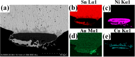
It can be seen that the solder joint formed by reflow at the peak temperature of 260 ℃ for the 20s left a blackened crater after a fracture. Only trace Au and Ni atoms were detected at the fracture, while Cu and Sn atoms were depleted. Sn and Cu may be consumed by IMC growth under the impacts of high temperature and long reflow time. If the reflow temperature continues to rise above 260 ℃, the pad will be further dissolved, and the risk of peel-off will increase.

Figure 4. Solder joint failure caused by peak refow temperature of 260 ℃ for 20s (Zhang et al., 2022).
Summary
A higher reflow temperature than 270℃ and a long reflow time will easily cause solder joint oxidation, resulting in more voids. The formation of voids seriously reduces the reliability of the solder joints. Besides, the pads will be further dissolved, reducing the shear strength of the solder joints. Therefore, Zhang et al. believed that the optimal reflow process temperature for fan-out packaging is 260 ℃ and 10s. Under this reflow parameter, the shear strength of SAC305 solder joints can reach 216.41N.
Shenzhen Fitech can manufacture lead-free medium-temperature solder pastes and low-temperature solder pastes, such as SnAgCu solder pastes, SnBiAg solder pastes, etc., which can replace ultra-fine-pitch BGA solder balls. Welcome to contact us for more information.
Reference
Zhang, S.Y., Duan, R., Xu, S.W., Xue, P.F., Wang, C.Q., Chen J.S., Paik, K.W. & He, P. (2022). “Shear performance and accelerated reliability of solder interconnects for fan-out wafer-level package”. Journal of Advanced Joining Processes, vol.5.


 Back to list


