Mini-LED Fan-out Panel-Level Packaging Solder Paste Test

https://en.szfitech.com/
Mini-LED Fan-out Panel-Level Packaging Solder Paste Test
As a new display technology, mini LED containing thousands of micro-LED chips has realized a wide color gamut and high contrast display, which has been applied in the large screen HD display industry. Mini LED display technology includes a direct display and backlight. The mini LED direct display is packaged with RGB chips, and the luminous function is realized by forming a P-N junction and applying current. The high chip density challenges the packaging difficulty. Fan-out packaging is applied to mini LED packages because it can provide more I/O terminals for the components and reduce LED spacing to less than 50μm. This article will introduce the performance of the mini-LED fan-out package.
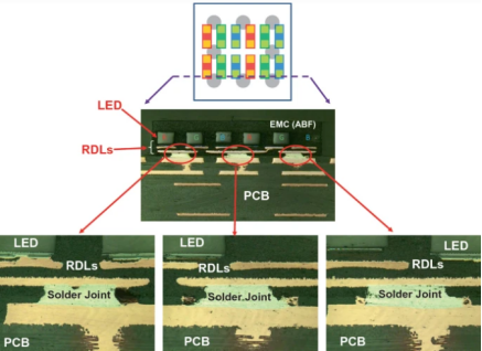
In order to verify the feasibility of manufacturing micro LED RGB display by fan-out panel-level packaging, Lau (2021) used 12 RGB chips grouped into 4 to produce a surface mount component (SMD) and conducted a soldering performance test. The spacing between mini LED chips was 80μm. Pixel-to-pixel spacing was 80μm. The specific parameters of the SMD are shown in Figure 1. SAC305 solder paste was printed on PCB, and reflow was completed to form solder balls. Then the SMD was placed on the PCB by pick and place method, and reflow soldering was completed (Figure 2).

Figure 1. Mini-LED RGB surface mount assembly.
Figure 2. SMD on the PCB and soldering result.
Drop Test
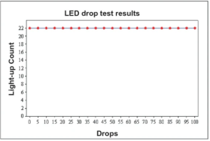
Lau selected a total of 22 samples for the drop test. The drop height was set at 648mm. The test result shows that all LED chips could still light up normally after 100 drops, indicating that the solder joints formed by SAC305 solder paste have good drop resistance performance and can meet the requirements of 100 drops. However, the Cu layer of the redistribution layer (RDL) had a crack formation, resulting in a loose connection between the LED chips and the RDL. Therefore, the design of the rerouting layer needs to be improved.

Figure 3. Numbers of light-up after 100 drops.
Thermal Cycling Test
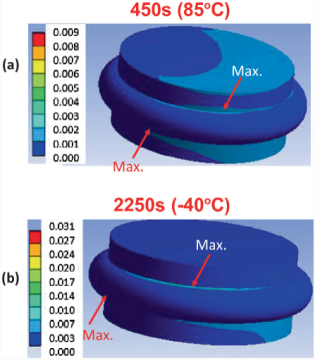
The temperature range of the thermal cycling test was set from -40-85 ℃. Each thermal cycle duration was 60 minutes. Lau found that the maximum accumulated creep strain of the solder joint was so small at 85°C. Only small areas were found to have slightly larger creep strain values. Similarly, the maximum cumulative creep strain was small when the temperature was -40℃. In addition, the accumulated creep strain rate was less than 1% for each thermal cycle, which verifies that SAC305 solder paste can maintain good creep resistance in mini LED fan-out panel-level packaging.

Figure 4. Cumulative creep of the soldered structures. (a): 85 ℃, 450s; (b): - 40 ℃, 2250s.
Shenzhen Fitech can produce ultra-fine solder paste products (T6 and above) for mini LED chip soldering, including printing-type SnBiAg low-temperature solder pastes and SnAgCu medium-temperature solder pastes, which can be used in different stages of multiple reflow soldering. After soldering, the electrical conductivity and mechanical strength of the solder joints are excellent, and the light attenuation of the chips is small.
Reference
Lau, J.H. (2021). “Fan-Out Panel-Level Packaging of Mini-LED RGB Display”. Semiconductor Advanced Packaging.


 Back to list


