Printing Solder Paste_ Electroforming Process for Stencil Manufacturing

Printing Solder Paste_ Electroforming Process for Stencil Manufacturing
Solder paste printing needs to be realized through a stencil. The stencil opening needs to be aligned with the substrate pad to achieve accurate printing. It can be said that the stencil quality has a significant impact on the printing effect. The influences of the stencil opening on the printability and release of solder paste cannot be ignored. If the apertures have burrs, the smooth printing of solder paste will be blocked. If the aperture walls are rough, the solder paste sticks to the wall during release, which makes the solder pad have insufficient solder volume and uneven solder shape. After reflow, it will lead to the thermal slump of solder joints and uneven solder joints. Different stencil manufacturing processes will bring different aperture wall quality.
At present, the most common stencil manufacturing processes include chemical etching, laser cutting, and electroforming. The stencil is mainly made of nickel and stainless steel. Nickel can provide better printability and is more widely used. Neither chemical etching nor laser cutting can form smooth aperture walls. An additional electropolishing process for the apertures is required. The stencil made by the electroforming process has the most uniform and smooth aperture walls, and the apertures made by the electroforming process are in the shape of an inverted trapezoid, which is conducive to the deposition and release of solder paste. The release quality of solder paste is particularly important for chips with ultra-fine sizes and pitches. The electroformed stencils can improve the release performance and achieve 95% solder paste transfer efficiency. In addition, electroformed stencils are also suitable for micro BGA processes, flip chips, and wafer bumps.

Figure 1. Stencil made by electroforming process.
Electroforming process
The electroforming process includes laying the photoresist film on the mandrel and covering the mask with the pattern of the pad on the dry film resist. Then the mold is exposed to ultraviolet light. The unformed dry film resist will strip off, leaving the imaging dry film resist on the mandrel. The mandrel is then immersed in a nickel bath and energized. This process is known as electroforming. Nickel atoms deposit on the mandrel along the current direction to form a nickel layer. Nickel atoms will be deflected by dry film resists and form a trapezoidal structure. Finally, the formed nickel is separated from the mandrel and the dry film resists, and a nickel stencil is produced.


Figure 2. Schematic diagram of electroforming process.
The electroforming process is difficult to control, and the cost is high. If the size of the pad is large, the stencil made by chemical etching and laser cutting can provide more economic benefits.
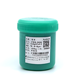
Shenzhen Fitech can provide solder paste products for the printing process. Fitech’s printing solder paste has adjustable viscosity, guaranteeing excellent printability and solder release performance. The products can help customers eliminate their concerns about the unstable printing performance of solder paste. Welcome to inquire for more information.


 Back to list


