Medium-Temperature Solder_ Thermal Fracture Failure Mechanism of BGA Solder Joints

https://en.szfitech.com/
Medium-Temperature Solder: Thermal Fracture Failure Mechanism of BGA Solder Joints
BGA has been widely used in high-density packaging to meet the demand for increasing I/O interfaces of integrated circuits. Compared with traditional microelectronic packaging technology, BGA uses alloy solder balls instead of pins to realize signal transmission, reducing the transmission loss of electrical signals. However, high-density integration also brings higher service temperature, which challenges the thermal aging reliability of BGA. Under the action of high temperature, thermal stress will continue to be generated inside the solder joint, leading to fatigue accumulation, which may eventually lead to solder joint fracture.
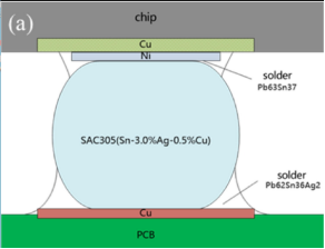
It is well known that the emergence of IMC is inevitable for lead-free soldering. Since the growth of IMCs in the aging process is the key factor to determine the reliability of solder joints, it is necessary to understand the microstructure changes of solder joints in the thermal fatigue process to infer the influence of IMCs on the reliability of BGA solder joints. As shown in Figure 1, Li et al. used medium-temperature SAC305 BGA to complete the assembly with Sn63Pb36 solder paste and Sn62Pb36Ag2 solder paste layers and carried out a thermal cycling test (- 55 ℃ - 125 ℃). The top of the SAC305 BGA is connected to the Ni pad of the chip, and the bottom is connected to the Cu pad of the PCB.

Figure 1. Schematic diagram of BGA solder joint.
BGA Solder Joint Aging Test Results
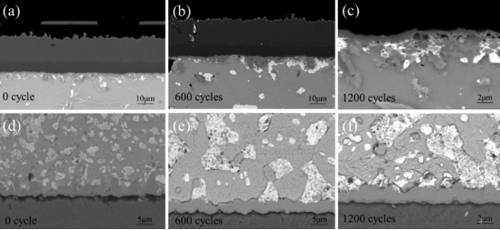
As shown in Figure 2, the gray zone of lead-free solder SAC305 BGA is Sn, and the white zone is Pb. When the soldering was just completed, the soldering grain structure was fine. After 600 thermal cycles, Pb continuously diffused into BGA, and Pb grains began to coarsen. In addition, after 1200 thermal cycles, further coarsening and accumulation of Pb grains to form a network structure can be clearly seen on both the BGA-chip side and the BGA-PCB side.

Figure 2. BGA solder joint aging test. (a-c) BGA-chip side; (d-f) BGA-PCB side.
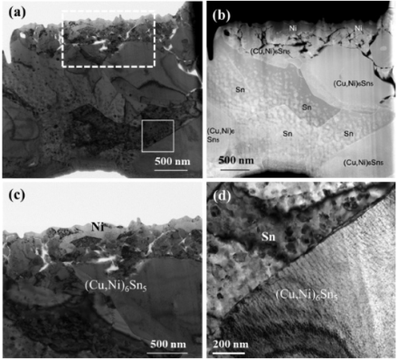
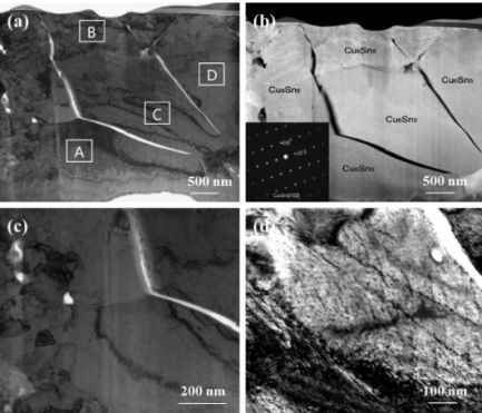
After 3200 thermal cycles, the BGA-chip side can be roughly divided into Ni zone, IMC (Cu, Ni) 6Sn5 zone, and Sn zone. Grain coarsening and recrystallization can be observed in the Sn region. In the (Cu, Ni) 6Sn5 region, dislocations occurred to some extent. In addition, on the BGA-PCB side, it can be seen that there are long cracks at the interfaces of the AC zone and BC zone. The cracks extended outward along the grain boundary (Figure 4), forming transgranular cracks. This brings hidden trouble of solder joint fracture. Figure 4(c) also shows the formation of voids. Under the combined action of voids and cracks, the fracture may occur more easily when the region is stressed. In addition, there will be grain dislocation in zone D on the BGA-PCB side.

Figure. 3. Microstructure of BGA-chip side after 3200 thermal cycles. (b) Composition distribution of Figure (a); (c) Enlarged view of dotted line area of Figure (a); (d) Enlarged view of the solid line area of Figure (a).

Figure 4. Microstructure of BGA-PCB side after 3200 thermal cycles. (b) Composition distribution of Figure (a); (c) Enlarged view of Zone A; (d) Enlarged view of Zone C.
Fracture Analysis of Solder Joint
The mismatch of thermal expansion coefficients of lead-free BGA solder joints, solder layers, and pads is the main cause of thermal aging failure of solder joints. When thermal stress is generated during the use of components, the expansion of materials arise the internal and surface stress of solder joints, which will gradually accumulate. Li et al. indicate that recrystallization of Sn grains and dislocation of (Cu, Ni) 6Sn5 can release partial stress. (Cu, Ni) 6Sn5 tends to diffuse to the Ni layer of the chip pad and form a grid structure, which can also release stress. It can be known that the Ni layer plays a role in inhibiting atomic diffusion, slowing down the growth of IMCs. Thus, the fracture failure rate decreases. However, there is no barrier of the Ni layer at the BGA-PCB interface, Cu6Sn5 grows faster, and transgranular cracks will appear under stress.
Shenzhen Fitech can produce medium-temperature solder paste products that can replace BGA solder balls for high-density and ultra-fine-pitch soldering. At the same time, the medium-temperature solder paste products can be used to deposit solder layers on the pads for solder ball planting. Welcome to contact us for more information.


 Back to list


