The Basic Knowledge of Lead-Free Solder Paste (5)_Shenzhen Fitech
The Basic Knowledge of Lead-Free Solder Paste (5)_Shenzhen Fitech
Continued from "The Basic Knowledge of Lead-Free Solder Paste (4)"
There are many kinds of solder joint defects that may occur after reflow solderings, such as Kirkendall voids, thermal creep, and electromigration. With the development of the miniaturization of electronic components, the size of solder joints is becoming increasingly miniaturized, and the defect of soldering leads to a larger area of voids. The Kirkendall void poses a great challenge to the solder joint reliability. Meanwhile, with the development of electronic technology, solder joints need to face various complex service temperature scenarios. Under the action of high temperature, thermal stress will be generated in the solder joint and lead to deformation of the solder joint. In addition, electromigration occurs in devices with high current density.
1. Kirkendall voids
1.1 Cause
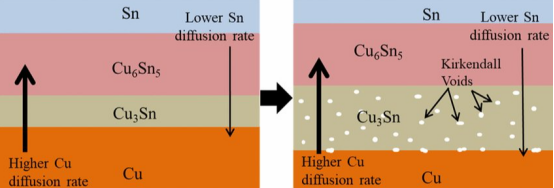
The kirkendalll effect is a common effect in lead-free solder paste soldering, which will affect the reliability of solder joints. The formation of Kirkendall voids is mainly caused by the difference in intrinsic diffusivity (nonreciprocal diffusion) of the solid solution components. In the process of thermal aging, the intermetallic compound layer of solder joints will grow continuously due to the influence of temperature. For example, solder joints made of SnAgCu lead-free solder paste will accelerate the diffusion of metal elements when heated. In Cu3Sn and Cu6Sn phases, Cu is a component that diffuses faster than Sn. The outward diffusion of Cu is faster than the diffusion of Sn to Cu (the atomic flux between Sn and Cu is unbalanced). Therefore, vacancies will be left inside Cu3Sn and at Cu3Sn/Cu interface. The continuous accumulation of vacancies will eventually develop into the Kirkendall voids.

Figure 1. The mechanism of void formation.
1.2 Impact and solutions of Kirkendal voids
The different thermal expansion coefficients of intermetallic compounds will cause internal stress. Under the action of stress, microcracks will gradually form near the solder joint cavity. With the further expansion of cracks under stress, brittle fracture is eventually caused. Since the appearance of voids will reduce the mechanical reliability of solder joints, the void ratio should be controlled in the range of less than 10%. At present, the industry mainly adopts the method of adding dopants to inhibit the formation of voids. For example, nickel is added to the lead-free solder paste to inhibit voids. The addition of nickel reduces the Cu3Sn layer thickness. For electroplated copper substrates, the doping of a small amount of nickel reduces the number of voids.
2. Thermal creep of lead-free solder paste
2.1 Cause
The thermal stress formed under high temperatures will be likely to cause thermal creep when it acts on components and solder joints. Solder joints are constantly affected by thermal cycles during use. Due to the mismatch of thermal expansion coefficients of electronic devices, substrates, and lead-free solder joints, stress is inevitably caused. With the increase in temperature, the atomic diffusion rate is increased, and the dislocations begin to move, leading to grain boundary slip and plastic deformation of the solder joints.
2.2 Thermal creep effect and solution
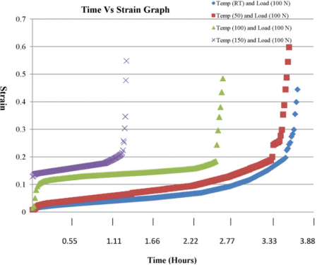
With the aging time increasing, the strain force at the solder joint will increase. When the working temperature increases and the load remains fixed, the solder joint will quickly deform and fracture. Similarly, under a low-temperature environment and high load, solder joints will still deform and fracture. It has been found that adding a small number of impurities such as Bi and Ni into the lead-free solder paste can reduce the dislocation movement of the tin-silver-copper lead-free solder paste and improve the thermal creep resistance.

Figure 2. The relationship between strain and time at different temperatures.
3. Lead free solder paste electromigration
Nowadays, the packaging density and interconnection number of electronic products are growing very fast, which greatly increases the current density. The current density is the main inducement of electromigration. Electromigration is the material migration caused by the momentum transfer between electrons and metal atoms under high current density. The increase of current density will generate joule heat inside the components. The temperature rises and accelerates the diffusion of materials, and the voids are generated on the cathode side, which eventually leads to the open circuit of solder joints.
Fitech is a world-leading provider of microelectronics and semiconductor packaging materials solutions. Fitech’s solder paste, epoxy solder paste, and other solder products have an outstanding wetting effect, narrow powder particle size distribution, and high post-soldering reliability. Welcome to the official website for more information.


 Back to list


