The Influences of Lead-Free Solder Voids on Flip-Chip LEDs
The Influences of Lead-Free Solder Voids on Flip-Chip LEDs
The void formation is a common problem in lead-free soldering. Gaps between lead-free solder paste particles can cause voids. Additionally, due to the inconsistent diffusion rate of metal elements, vacancies are usually left in the intermetallic compound layers, which will grow into voids after continuous aggregation. The appearance of voids affects the conductivity and thermal properties. Moreover, solder joints will have significant void growth after thermal aging, which increases the risk of failure. So how to quantify the effect of voids on the performance of solder joints?
The melting point temperature of SAC lead-free solder paste is about 217 ℃, so it is considered to be a more suitable connection material for flip chip LED. Liu et al. (2014) adopted SAC305 lead-free solder paste to conduct the packaging of DA3547 LED. Liu et al. analyzed how the volume of solder paste affected the formation of voids in LED chip packaging and explained the influences of the void ratio on thermal and mechanical properties.
1. Effects of lead-free solder paste volume on void growth
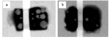
X-ray observation showed that the appropriate increase of lead-free solder paste volume significantly reduced the void ratio of the solder paste layer. After calculating, the void ratio of LED chip samples a and b were 46% and 3%, respectively (Figure. 1). Insufficient lead-free solder paste will lead to more voids between solder particles, which are easy to aggregate into voids after soldering. Therefore, the appropriate increase of solder paste content has a positive effect on reducing the void rate.

Figure 1. X-ray images of solder paste layers. (a)20μm thickness (b)30 μm thickness.
2. Impacts of voids on LED packaging
The shear strength of LED packaging is directly related to the void ratio. A large number of voids will reduce the effective soldering area and increase internal stress. The reduction of the effective area means that the stress will be more concentrated, which will significantly weaken the mechanical strength and increase the risk of fracture. When the void ratio is 46%, the shear strength of the LED chip is only about half of that of the chip with a 3% void ratio. A large void ratio will also increase the temperature of LED chips. Liu et al. found that the temperature of LED chips with a large void ratio is 40.5°C. The operating temperature of LED chips with a small void ratio is only 36.9°C. It can be concluded that the increase in the void ratio also harms the heat dissipation of the chips. The reason is that the large void ratio will lead to an excessive concentration of heat. The solder cannot effectively dissipate the heat, resulting in high temperature.

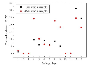
Figure 2. Thermal resistance of LED chip package with different void ratios.
Liu et al. calculated the thermal resistance and found that when the void ratio of the LED chip package is too large, the thermal resistance of each layer is generally large. Only in PI and TIM layers, the thermal resistance of the small void ratio chip is significantly greater than that of the chip with a large void ratio. In general, the thermal performance of chips with a small void ratio should be better.
Fitech can produce SAC305 lead-free solder paste that is suitable for LED packaging. The void ratio after soldering can be controlled within 10%. The solder joints have excellent mechanical strength, outstanding conductivity, and thermal conductivity. SAC305 lead-free solder paste is suitable for medium-temperature packaging scenarios. Welcome to the official website for a consultation.


 Back to list


