Introduction to Package on Package (PoP) and Pad Printing_Fitech Solder Paste

Introduction to Package on Package (PoP) and Pad Printing_Fitech Solder Paste
1. What is package on packaging (PoP)
With the development of semiconductor-integrated technology, the electronic products in the current market, such as mobile phones, computers, and electronic watches, are small and portable, with excellent electrical performance and low prices. The development of packaging technology is one of the key factors to improve performance and reduce the price of electronic products. PoP is an effective solution for chip packaging. PoP is made by overlaying two or more packages vertically, which is essentially a 3D overlay technology.
The bonding between PoP layers is completed by the use of BGA solder balls. The solder balls can realize the electrical and thermal paths between layers. There can be many types of packages for the PoP product. The bottom package can be a processor, and the package placed on the processor can be a memory.

Figure 1. An example of POP structure.
2. Pad printing process of solder paste
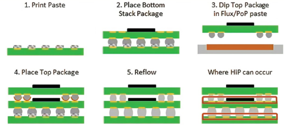
In order to fix the BGA solder balls on the PoP PCB, the printing process of transferring the solder paste to the PCB to form a thin solder paste point can be adopted, and then the solder balls of the bottom package are mounted precisely onto the solder paste point. The BGA on the PCB is called the lower BGA, while the BGA connecting the upper package and the lower package is called the upper BGA. It should be noted that the surface pads between the upper BGA and the lower BGA cannot be printed with solder paste. Therefore, the pad printing process is required. During the pad printing process, the upper BGA is directly dipped in the solder paste or flux, and then the upper BGA is mounted on the lower BGA at one time to complete the pad printing and mounting. After the bottom package and upper package are assembled, the whole package can be sent to the reflow furnace for soldering.

Figure 2. PoP assembly process.
3. Important notes for PoP assembly
(1) The viscosity of solder paste for dipping is low (~50Pa.s). The printing solder paste is not suitable for the PoP pad printing process due to its high viscosity.
(2) The height of solder paste/flux on the upper BGA of the PoP needs to be adjusted according to the real situation.
(3) The SMD machine should be able to identify the BGA that is dipped with solder paste/flux.
(4) The upper BGA needs to maintain high accuracy of the mounting position.
(5) To control the mounting pressure and height.
4. PoP solder paste
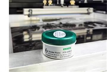
The printing solder paste products produced by Shenzhen Fitech include low-temperature, medium-temperature and high-temperature series. Customers can select the appropriate solder paste products according to the actual soldering temperature. Fitech’s solder pastes have the advantages of stable viscosity, long stencil on-board life, and high mechanical strength. Welcome to contact us for cooperation.


 Back to list


