Relationship between IGBT Heat Conduction and Solder Voids_Shenzhen Fitech

Relationship between IGBT Heat Conduction and Solder Voids
As an electronic component commonly used in high-temperature applications (automobiles, railway networks, aerospace, etc.), IGBT needs to withstand the impact of high-temperature aging. Solder paste is the material used for IGBT soldering, and it is also one of the most vulnerable parts in the multi-layer structure of the IGBT module. The soldering performance directly affects the chip temperature and device performance. The reflow soldering process and the growth of intermetallic compounds will produce voids in the solder joints. The appearance of voids will affect the heat conduction and the temperature distribution of IGBT chips.
Effect of voids on heat conduction
In order to understand the effect of voids on the heat conduction of IGBT, Fan et al. packaged the IGBT chip and the diode chip together and tested the temperature of different void areas. As can be seen from Figure 1, the voids between the IGBT and the diode solder joint caused a significant change in the central case temperature distribution.

Figure 1. Effect of voifs on the case temperature distribution of IGBT and diode.
The distribution of voids will affect the chip temperature. It can be found that the base solder voids at the edge slightly affected the chip junction temperature can be almost ignored (area a and area c), but the voids near the IGBT and diode (area b and area d) led to a significant increase of junction temperature. The voids in area b and area d increased the junction temperature of the IGBT and diode by nearly 6°C. It can be seen that when the voids appeared at the center of the chip, the junction temperature at the chips increased significantly. In addition, the voids reduced the heat flow and caused the shell temperature to decrease.
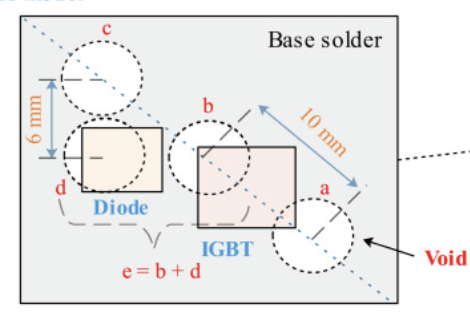

Figure 2. Junction temperature distribution of IGBT and diode chips.
The mechanism of cavity affecting heat conduction
The appearance of voids can increase the angle of thermal diffusion and the thermal resistance, slowing down heat conduction. When there is void formation under the chips, the thermal diffusion angle increases, which increases the heat transfer area and reduces the thermal resistance under the voids. Voids will influence both self-thermal diffusion and mutual coupling. If the diode chip size is smaller than that of the IGBT, the coupling thermal resistance between the diode and the IGBT is more susceptible to voids than that between the IGBT and the diode. In addition, the influence of solder voids on chip junction temperature and shell temperature is cumulative. If the shell temperature changes at multiple points, the coupling temperature is more likely to rise, which will more easily lead to IGBT module failure.
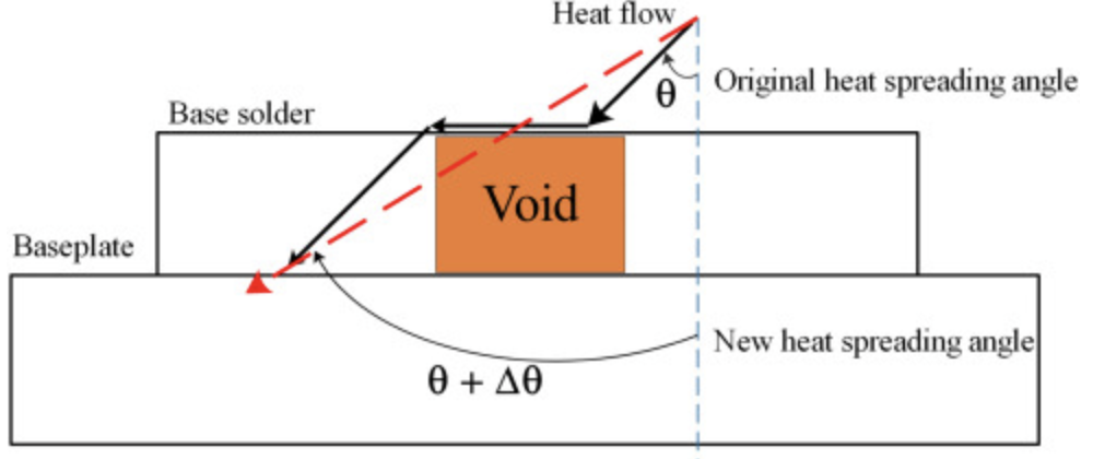
Figure 3. Relationship between thermal diffusion angle and void.
Solder materials with low void ratios
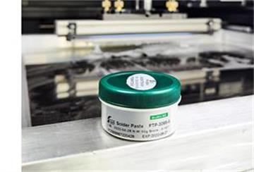
Shenzhen Fitech can produce ultra-fine solder paste products (T6 and above) with high reliability. Fitech’s solder paste products can be used for the soldering of various electronic components, such as IGBT, with a low void ratio and high mechanical strength and can provide stable electrical and thermal conduction. Welcome customers to contact us for more information.
Reference
Fan, Y.H., Cui, H.Y., Lou, Z.B., Teng, J.J., Tang, Z. & Peng, J.Z. (2020). Base solder voids identification of IGBT modules using case temperature. Microelectronics Reliability, vol.115.




 Back to list


