The Solder Joint Void Caused by Electroplating Impurity_Shenzhen Fitech

The Solder Joint Void Caused by Electroplating Impurity - Shenzhen Fitech
Voids are usually observed during reflow soldering, which is generally considered to be one of the reasons for weakening the thermal conductivity and mechanical strength of solder joints. When analyzing the cause of void formation, we can easily associate it with flux. The solvent evaporation and organic acid reaction of flux will form bubbles. The accumulation of bubbles that cannot escape will form voids. There is another type of void called Kirkendall void, which is caused by diffusion rate mismatch of solder components. The influence of soldering substrate impurities on void formation is often ignored.
Impurity effect experiment
Electroplating copper is a widely used process for preparing substrates. When using the electroplating process to prepare the copper substrate, impurities (carbon, sulfur, chlorine, etc.) may be mixed into the electroplating copper substrate. In order to understand the influence of impurities on the formation of voids, Hsu et al. soldered Sn solder balls on the electroplated copper substrate at 260 ℃. The preparation of electroplating copper substrates requires the use of copper foils and electroplating additives (PEG+Cl-). After soldering, Hsu et al. placed Sn/Cu solder joint samples in the furnace at 120, 150, and 200 ℃ for the aging test and then observed the microstructure of solder joints.
Experimental result
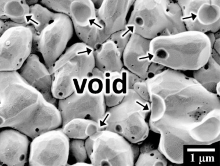
Cu6Sn5 will be formed at the interface between the Sn ball and Cu substrate during soldering and gradually grow during aging. Electroplating impurities often evaporate into the solder/substrate interface during the aging of the solder joints, thus occupying the position of Cu6Sn5 and turning into voids. As shown in Figure 1, voids with different sizes appeared on the surface of grains. When the solder joints are aging, the voids at the grain boundary will hinder the migration of the grain boundary and reduce the accumulation of grains. Similar to the Kirkendall voids, the voids caused by impurities will also make the solder joint brittle.

Figure 1. The SEM image of electroplating PC-Cu.
In order to determine whether the flux will affect the voids of the electroplating PC-Cu, Hsu et al. also adopted the flux-free process for soldering. The result showed that there was still a number of voids on the surface of Cu6Sn5. Therefore, it can be considered that the flux was not the main reason for the formation of electroplating PC-Cu voids.

Figure 2. The schematic diagram of electroplating additive impurities entering solder.
Iow-void solder pastes
Fitech has designed a reliable flux formula for high-quality ultra-fine solder paste production (T6 and above). The solder pastes have excellent wettability, low void ratio, and high solder joint strength that can be used for soldering with small spacing. Welcome to contact us for cooperation.


Reference
Hsu, H.L., Lee, H., Wang, C.W., Liang, C.J. & Chen, C.M. (2019). Impurity evaporation and void formation in Sn/Cu solder joints. Materials Chemistry and Physics, vol.225, pp.153-158.


 Back to list


