LGA device soldering failure analysisand countermeasures-Fitech Solder Paste

LGA device soldering failure analysisand countermeasures-Fitech Solder Paste
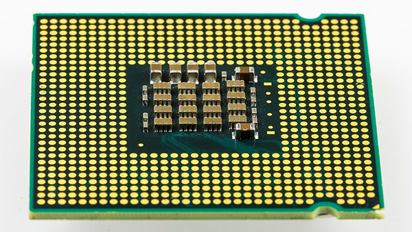
LGA (Land Grid Array) is the use of the device body pad as the solder side of the components, under the BTC device, and QFN similar. LGA has no pins and solder balls, and is susceptible to device and PCB deformation, as the body covers the solder, making it difficult for bubbles to escape from the solder joint and increasing the likelihood of bubbles.

Inspection of LGA solder joint quality usually requires the use of X-ray, 5D X-ray or 3D X-ray, with 3D X-ray (CT) inspection being the most intuitive and effective.
LGA device failure types
For LGA devices, the common failure problems are mainly short circuit and solder joint bubbles. These problems are related to the heavier devices; solder joint bubbles have a wide variety of causes, from device characteristics leading to voids are mainly caused by BTC devices.
Process Difficulties and Failures of Super Heavy LGA Devices
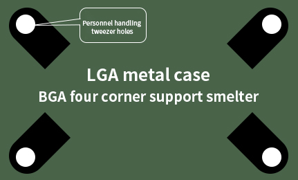
Some LGA devices are heavy, even with metal cases. Under the effect of gravity, the melted solder is squeezed by the body of the device, resulting in the solder suffering from excessive surface tension, which is not conducive to the escape of air bubbles from the solder joint, which in extreme cases can lead to short circuits. Designing the right support in the SMT process can alleviate this problem, and the industry usually uses two solutions: dispensing and jigging.
Dispensing refers to the use of automatic dispensing machine before SMT to apply the right amount of glue on the PCB, the glue in the reflow process first melted with the solder and hardened to help support the LGA device body; adhesion should be large, can play a complementary function of the solder joints, especially the LGA corners. The adhesion force should be high, which can play the function of reinforcing the solder joints, especially the LGA corners.
Jig is suitable for multi-species small batch enterprise, by placing jig in the corresponding four corners of PCB before LGA placement, then device placement and reflow soldering.

LGA solder joint cavity impact and control solution
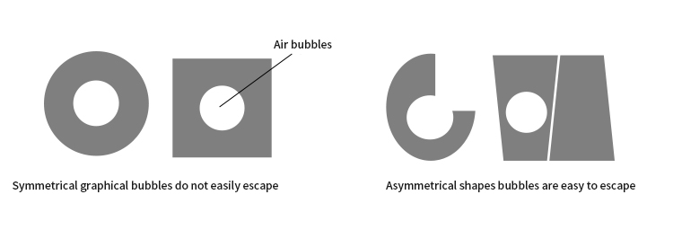
In order to control the problem of LGA solder joint voids, it is necessary to strictly follow the IPC-7095 specification. From the soldering principle, the bubble escape within the solder joint requires the smaller the solder area the better, the thinner the solder the better for bubble escape, and the lower the surface tension of liquid solder the better. However, from the viewpoint of solder paste printing shape and bubble escape, asymmetric graphics solder melting on the solder joint bubble imbalance in force, conducive to the escape of bubbles.

LGA pad design requirements
LGA welding characteristics are prone to air bubbles, while the BTC device welding characteristics are obvious - PCB deformation has a significant impact on the welding effect. Square pads and round pads can be used, pay attention to the surrounding and corner pad design needs to be increased, if conditions allow, the four corners set mechanical enhancement pad to strengthen the welding effect, to prevent the four corners of the solder joint by mechanical stress cracking and PCB & parts bending and twisting caused by empty welding. Prohibit the process of half plugging the hole in the disk to avoid the blind hole effect resulting in giant bubbles and poor plugging of the hole resulting in bubbles in the solder joint.
Fitech Ultra-fine Solder Paste
Shenzhen Fitech has rich experience in producing printing solder paste, and can provide customers with ultra-micro printing solder paste products with stable viscosity and excellent printing performance. The solder joints formed during reflow soldering have high strength and few voids, which can meet high reliability requirements.


 Back to list


