Common PCB solderability inspection methods-Shenzhen Fitech

Common PCB solderability inspection methods
PCB solderability inspection method refers to the use of certain methods and standards to evaluate the solderability of the pads or components on the PCB, that is, the wettability and interfacial reactivity between the solder and the solder. The international standard J-STD-003 specifies that PCBs need to be tested for solderability before shipment.
Solderability is an important factor affecting the reliability and quality of PCB, if poor solderability, will lead to weak, incomplete and uneven solder joints, and even defects such as false solder and broken circuit. Therefore, the PCB solderability inspection is necessary to find and solve problems in time to improve the manufacturing level and service life of the PCB.
Common solderability inspection methods are:
Solder Balance Experiment Method
This method evaluates the solderability by measuring the wetting force of the solder on the component leads or pads. Wetting force is the adhesion force between the solder and the solder, which reflects the degree of interface reaction between the solder and the solder. The greater the wetting force, the better the solderability. Wetting force can be measured with an instrument called a wetting equilibrium meter. A wetting balance meter can plot a wetting curve showing the change in wetting force over time. The shape and area of the wetting curve can be used to determine the goodness of the solderability.
Tin bleaching experimental method
The PCB to be tested is dipped into the flux tank for 30 seconds, fished out and put into the molten tin tank at an angle of 45 degrees to maintain 5 seconds (note that the test sample should not be swung within the solder during the immersion time), fished out and observed the solder surface. When more than 95% of the area of the tin surface is uniformly smooth and well wetted, the remaining area is not concentrated pinholes, back wetting, surface roughness and other defects, it means that the solderability is good.

Printed tin experimental method
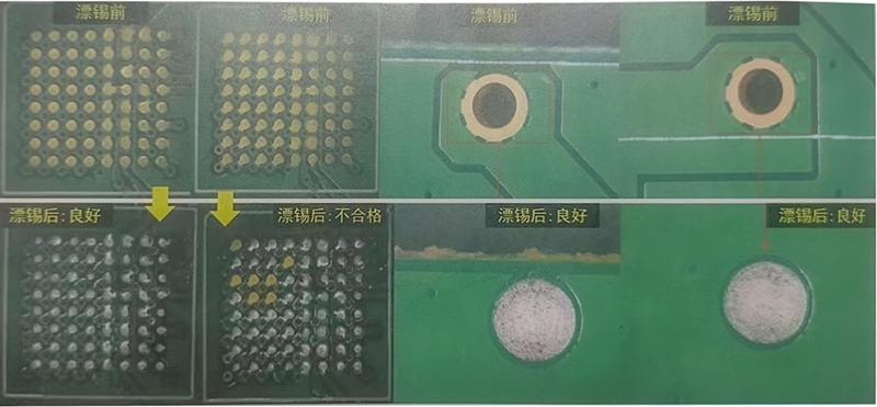
Printed tin test is another commonly used to assess the PCB solderability program, because PCB manufacturers generally do not have PCBA process equipment, is mostly used in SMT factories to assess the PCB solderability. With the trend of portable electronic products thrive, HDI board applications become mainstream, such as cell phones, tablet PCs, notebook computers and other portable products manufacturers have not used wave soldering process for many years, the factory naturally can not be used to do bleaching tin experiments wave soldering equipment, which allows the use of printed tin experiments to identify PCB solderability a show, shine.
Printed tin experiment is the use of PCB corresponding SMT printing process steel plate normal completion of solder paste printing, directly over reflow (normal reflow process parameters) after observing the PCB pad solder wetting conditions to determine the PCB pad solder performance. HDI board soldering process only T & B side two thermal shock, considering the pad surface alloying and baking and other factors, the general requirements of the new PCB bare board Directly over the reflow once before doing the printed tin experiments. Another gain of the printed tin experiment is to verify the suitability of the steel plate opening design, to have an extended foot device, for example, after the printed tin experiment solder uniformly laid flat on the pad is not the most perfect state - different liquid surface tension, the unit area can carry the amount of this liquid is fixed, the amount of solder required for the device pins in the absence of pins When the pads will be stacked on the pad and the formation of tin tumor, melting after the tin tumor of the steel plate open hole design is actually the tin amount is not sufficient performance.
Printed tin experiments can accurately evaluate the actual PCB solderability, as opposed to wave soldering bleaching tin experiments and tin bath bleaching tin experiments, the process is a bit complicated, but its direct effect is increasingly being endorsed by industry colleagues and use.
Tin dragging experiment method
Solder dragging experiment is the oldest practice of manual use of soldering iron to assess the PCB solderability, in the initial manual soldering stage increased to the mainstay. Soldering iron dragging tin is generally sufficient solder, the formation of a full solder joint, but also therefore conceals the phenomenon of PCB rewetting, which is not conducive to determining the wetting angle of the solder joint. Pile up of solder to cover part of the phenomenon of shrinking tin, which is similar to BGA solder joints many solder balls soldering normal, a ball corresponding to the pad not on the tin will still form a drum-shaped solder joints. This is why the industry assesses a solder joint to see the wetting angle rather than the reason for the amount of tin, but also one of the reasons why international first-class car companies do not accept manual welding. Another factor affecting manual drag welding is the higher temperature of the soldering iron, higher flux content of the wire, which makes the normal reflow & wave soldering process soldering bad people in the drag welding still have the opportunity to be covered with solder leads to misjudgment of PCB solderability. With the evolution of the industry process and product reliability requirements to enhance the manual drag welding gradually into history and be dusted.


 Back to list


