PCB surface treatment - Introduction to the OSP process-Shenzhen Fitech

PCB surface treatment - Introduction to the OSP process
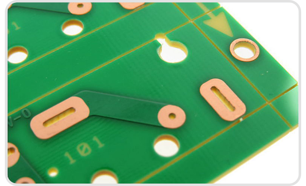
PCB surface treatment is to cover the PCB surface with a protective layer to prevent copper oxidation, corrosion and to improve solderability, reliability and aesthetics. there are various PCB surface treatment processes, such as tin spraying, gold sinking, silver sinking, etc., of which OSP is an environmentally friendly process that meets the requirements of the RoHS directive.
What is OSP?
OSP is the abbreviation for Organic Solderability Preservatives, also known as bare copper, Entek. simply put, OSP is an organic skin film that grows chemically on a clean bare copper surface. This film is resistant to oxidation, thermal shock and humidity and protects the copper surface from further rusting (oxidation or sulphidation etc.) in the normal environment; however, in the subsequent high soldering temperatures, the film must be easily and quickly removed by the flux so that the exposed clean copper surface can be immediately bonded to the molten solder in a very short time.
There are three main types of OSP materials: rosin, active resins and azoles. Currently the most widely used is the azole OSP.

OSP process flow
1. Pre-treatment: The PCB is cleaned, degreased and micro-etched to remove dirt, grease and oxides from the surface, increase the surface roughness and improve the adhesion of the OSP film.
2. Film formation: The PCB is dipped into a solution containing azole compounds and other additives to allow the azole compounds to react on the copper surface to form a transparent, dense and uniform organic solder film.
3. Post-treatment: The PCB is washed and dried to remove residual solutions and impurities and to increase the gloss and flatness of the solder retention film.
What are the advantages and disadvantages of the OSP process?
Advantages | Disadvantages |
Environmentally friendly, no harmful elements such as lead | Fragile, easily scratched or scuffed |
Good solderability, can be matched to any type of solder | Poor testability, not easy to measure and observe |
High flatness, suitable for high density and fine pitch PCBs | Poor compatibility, reacts easily with fluxes in solder paste |
Good stability, prevents oxidation and corrosion of copper | Film thickness difficult to control, affecting reliability and solder resistance |
Economical, simple, fast and cost effective process | Short shelf life, requires strict control of packaging and storage conditions |
The following requirements need to be observed during the use of OSP plates:
1. the effective service life of the OSP board should be completed within 48H/72H (according to PCB factory specifications).
2. OSP boards must not be baked, as baking will cause the OSP film to crack and lose its protective capacity.
3. OSP boards must not be cleaned, solvent cleaning and water-based cleaning agents will dissolve the OSP film and lead to loss of protection.
4. OSP boards should be used in an environment that follows the requirements of the industry: control the temperature and humidity values, PCBA workshop temperature and humidity control range is generally 28+3℃ (or 18~28℃), 40%RH~60%RH (some companies control at 40%RH~70%RH).
5. The OSP board should be cleaned with a small hand-held scraper to remove the solder paste, then wipe with wiping paper or dust-free paper (do not dip into solvent) or tape bonding to clean up, and finally use the pressure air gun to clean up, and put into use after microscopic inspection to confirm OK.
6. Long-term storage of OSP board or expired OSP use need to be returned to the PCB factory to remove the film, pickling, Recoating and then put into use. However, attention should be paid to the control of the pickling of the copper foil of the solder pads, as the thinning of the copper foil caused by excessive pickling has an impact on the reliability of the product.
In short, OSP board surface treatment is low cost, superior performance, its soldering to form copper, tin intermetallic compounds, bonding strength, is the industry's early use and widely used surface treatment solutions, and is still widely used.


 Back to list


