PCB Copper Pad Corrosion Caused by Solders - Fitech Solder Paste

PCB Copper Pad Corrosion Caused by Solders - Fitech Solder Paste
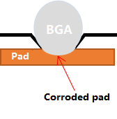
When a PCB is wave soldering or reflow soldering, the solders will corrode the copper pads. Solder pad corrosion is mainly reflected in the reduction of PCB copper pad thickness. One of the causes of copper pad corrosion is the corrosion effect of tin-based solders on copper pads. As the diffusion of Sn and Cu accelerate under high-temperature soldering, the Cu atoms on the pad will gradually dissolve into the Sn based solder, resulting in the shrinking pad thickness. Diffusion is a continuous process, which means that if the soldering time increases, higher amount of Cu will diffuse into the solder matrix. If the corrosion resistance of the copper pads is low, it is likely to arise the copper layer reduction problem. Furthermore, the wet manufacturing process and surface finish process in PCB production may corrode the copper pads.

Figure 1. The copper pad is corroded by a solder ball.
In order to detect the PCBs with poor corrosion resistance and avoid the excessive corrosion issue of pads during soldering, the industry proposed PCB copper corrosion test. The purpose of copper corrosion test is to understand the resistance of PCB copper pad to the solder corrosion at high temperature, and to analyze whether the performance of PCB materials and manufacturing process are abnormal. In addition, the influence of pad thickness reduction on solder joint reliability can be analyzed through copper corrosion test.
Scope of application: all electronic devices involving PCBs as substrate carriers.
3.1 Copper corrosion test after reflow soldering
l The first step is to select two bare PCBs and print the solder paste on the bonding pads. After printing solder paste, the PCB should be sent to reflow for two times. The detection area can be plated thrpugh holes, BGAs, QFPs, SMT devices, etc;
l To slice the PCBs and measure the copper pad thickness or the copper thickness of the the through-hole walls;
l To compare the measured PCB pad thickness/through-hole copper thickness with the specifications.
3.2 Coppre corrosion test after wave soldering
l The first step is to select two bare PCBs. The detection area can be plated thrpugh holes, blind vias, etc;
l To slice the PCBs and measure the copper thickness at the chosen detection areas;
l To compare the measured copper thickness with the specifications.
After the PCB copper corrosion test is completed, qualified PCBs can better perform SMT and other following processes. When the manufacturer prepares for the subsequent SMT process, Shenzhen Fitech can provide the corresponding ultrafine printing solder paste products (T6 and above) for component package. Fitech’s ultrafine printing solder paste has excellent solderability and wettability, which can be reliably combined with PCB pads after soldering. Welcome to contact us for more information.


 Back to list


