Solder Joint Reliability with Different Reflow Number - Shenzhen Fitech

Solder Joint Reliability with Different Reflow Number
Flip-chip packaging has a shorter electrical path length than wire bonding, which allows it to provide excellent electrical performance, high input/output density, and high interconnection speed. However, the cost of the flip-chip process is much higher than that of wire bonding. Therefore, some researchers proposed to combine maskless chemical wafer bump technology with ENIG electroplating and stencil printing process to reduce under bump metallurgy (UBM) sputtering and photolithography. As a result, the high-cost problem of the flip-chip process can be solved.
After the solder paste is printed on the wafer, a reflow process is conducted to produce micro bumps. The reliability of micro bumps is a topic worthy of attention. Ha et al. evaluated the mechanical strength of SAC305/Sn63Pb37 solder bumps on the ENIG UBM. The flip-chip device adopted ENIG surface finish with Ni-P layer and Au layer thicknesses of 6μm and 0.15μm, respectively. The pad diameters were 80μm, 100μm, and 130μm. The peak reflow temperatures of Sn63Pb37 and SAC305 solder pastes were 225°C and 255°C, respectively.
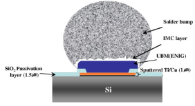
Figure 1. Schematic diagram of flip chip solder joint.
The diameters of the solder bumps after reflow were 130μm,160μm, and 190μm. During reflow, Au in the ENIG layer was first dissolved into the solder. For Sn63Pb37 solder paste, the Ni3Sn4 IMC layer was formed at the interface between the solder and Ni-P UBM due to the fact that Ni diffused from the Ni-P layer and reacted with the solder matrix. Furthermore, the IMC of the as-reflowed Sn63Pb37 bump was thinner, and the IMC layer became thicker with the increase in reflow number.
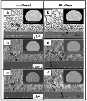
Figure 2. Sn63Pb37/ENIG interface after reflow: (a, b) pad size 130μm; (c, d) Pad size 100μm; (e, f) Pad size 80μm.
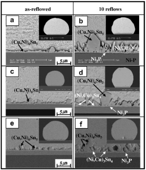
Figure 3. SAC305/ENIG interface after reflow: (a, b) pad size 130μm; (c, d) Pad size 100μm; (e, f) Pad size 80μm.
(Cu, Ni) 6Sn5 was formed at the interface between the as-reflowed SAC305 solder paste and the Ni-P layer. With the increase of reflow number, the IMCs of (Cu, Ni) 6Sn5 and (Ni, Cu) 3Sn4 wer5e formed at the interface between the as-reflowed SAC305 solder paste and the Ni-P layer. Besides, it is clear that the thickness of IMC increased with the increase in reflow number.
When using the flip-chip device, it is inevitably affected by various mechanical loads and thermal stresses. Therefore, the reliability of chip bumps is important. Ha et al. found that there was no significant relationship between the change of bump shear force and the number of reflows. The sheer force of large-sized bumps was higher than that of small-sized bumps. In addition, the shear force of the SAC305 bumps was greater than Sn63Pb37. After the shear test, the fracture mode of as-reflowed Sn63Pb37 bumps and the Sn63Pb37 reflowed 10 times was both ductile fracture. The as-reflowed SAC305 bumps were a ductile fracture, but a partially brittle fracture occurred after 10 reflows.
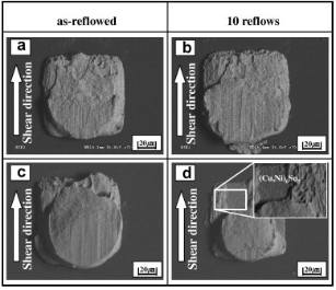
Figure 4. Bump failure surface after shearing: (a, b) Sn63Pb37; (c, d) SAC305 (pad size 80μm)。
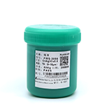
Shenzhen Fitech can manufacture medium-temperature ultrafine solder pastes (T6 and above) for the processes such as SMT and bump formation. Fitech’s medium-temperature solder paste (such as the SAC305 series) has excellent printability and solderability that can be smoothly printed on the substrates. The solder joints formed after the reflow are uniform and have excellent mechanical strength. Welcome to inquire for more information.
Click here for more Fitech's products>>
Reference
Ha, S.S., Kim, D.G., Kim, J.W., Yoon, J.W., Joo, J.H., Shin, Y.E. & Jung, S.B. (2007). Interfacial reaction and joint reliability of fine-pitch flip-chip solder bump using stencil printing method. Microelectronic Engineering, vol.84, pp.2640-2645.




 Back to list


