High-Temperature Gold-Tin Solder Bump Fabrication and Reliability_Shenzhen Fitech

High-Temperature Gold-Tin Solder Bump Fabrication and Reliability
At present, there are about three types of solder paste products that are the most common and mature in the packaging solder industry. One is low-temperature SnBi57.6Ag0.4 solder paste (melting point ≈138℃). Another is medium-temperature SAC305 solder paste (melting point ≈ 217℃). There is also Sn90Sb10 solder paste (melting point ≈ 245℃), which can meet the requirements of a higher melting point. In order to achieve much higher melting point requirements than Sn90Sb10 solder paste, gold-tin solder was invented in the packaging material industry. Eutectic gold-tin solder (Au80Sn20) has a melting point of 280℃, which can be used in some electronic products requiring high soldering and operating temperature, such as high-power electrical appliances, aerospace equipment, etc. Gold-tin solder coating methods include preforms, solder paste printing/dispensing, electron beam evaporation, and solder electroplating.
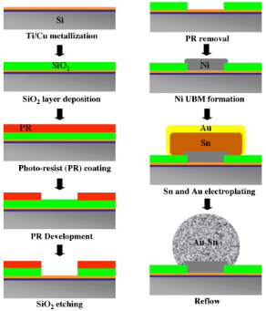
Gold-tin solder electroplating is a very attractive solder coating method, which has the advantages of low cost, fast speed, and easy control. The electroplating process is to use separate Sn and Au solutions to successively plate Sn and Au layers on a substrate. In order to avoid too fast diffusion of Cu atoms in the bonding pad, Ni can be used as the under bump metal (UBM) on the Si wafer. After electroplating, reflow is carried out to form micro bumps. The complete process of electroplating gold-tin solder is shown in the figure below.

Figure 1. The preparation process of micro-punch preparation of gold-tin solder.
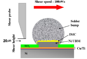
Yoon et al. first metalized Si wafers with Ti/Cu then deposited the SiO2 passivation layer and prepared Ni UBM. Finally, Sn and Au electroplated layers were prepared separately on Si wafers, and reflowed was conducted to generate Au-Sn solder bumps. The bumps were subjected to aging and shear tests. For the aging test, the samples were aged for 1000 hours at 150℃. Besides, the shear speed and shear height of the shear test was 100μm/s and20μm, respectively.

Figure 2. The schematic diagram of bump shear test.
Yoon et al. observed by SEM that the intermetallic compounds (IMC) of gold-tin bumps mainly consisted of Au5Sn (light gray) and AuSn (dark gray) after aging at 150℃. Due to the high solubility of Ni in AuSn, Au-Ni-Sn compounds were formed at the interface of Ni UBM. In addition, it can be clearly seen that the thickness of IMC increased with aging time. When aging time increases, a large amount of AuSn is deposited above the Au-Ni-Sn compound.

Figure 3. The SEM diagram of Au80Sn20/Ni interface after aging at 150 ℃ for different time. (a)0h, (b)48h, (c)100h, (d)250h, (e)500h, (f)1000h。
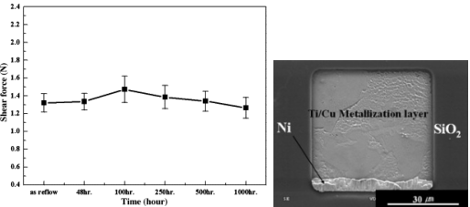
The aging time has no significant effect on the shear stress of Au-Sn solder bumps. The bump shear force showed an upward trend from as-reflowed until 100 hours of aging. With the further increase of aging time, the shear force decreases slightly. The shear fracture surface shows that the fracture failure mainly occurred at the interface between Ti/Cu and Ni UBM. Therefore, the strength of Au-Sn solder was higher than the bonding strength of Ti/Cu and Ni UBM, representing that the gold-tin solder had excellent reliability.

Figure 4. The change of shear force at bump and the fracture surface after aging for 1000 hours.
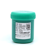
Instead of the solder electroplating method, the eutectic gold-tin alloy can be fabricated into solder paste that can be printed or dispensed on the substrate. Shenzhen Fitech has rich experience and advanced production technology support in the production of Au80Sn20 solder paste. The Fitech’s FH-280 gold-tin solder paste has a melting point of 280℃and has stable printability/dispensing performance. Moreover, the FH-280 product has excellent mechanical strength and conductivity after reflow soldering. Welcome to contact us for cooperation.
Yoon, J.W., Chun, H.S.& Jung, S.B. (2008). Reliability evaluation of Au–20Sn flip chip solder bump fabricated by sequential electroplating method with Sn and Au. Materials Science and Engineering: A, vol.473(1-2), pp.119-125.


 Back to list


