Microstructure Evolution of Eutectic Gold-Tin Solder Joints- Shenzhen Fitech

Microstructure Evolution of Eutectic Gold-Tin Solder Joints- Shenzhen Fitech
When it comes to lead-free solder pastes, many people are familiar with medium-temperature SnAgCu solder pastes and low-temperature SnBiAg solder pastes. Both types of lead-free solder pastes have a wide range of applications, and their melting points range from 139℃ to 217℃, which can meet most conventional packaging requirements. However, some areas require high-temperature solders. Since the use of leaded solder paste is restricted, as a substitute for high-temperature leaded solder paste, eutectic gold-tin solder paste (Au80Sn20) has been developed for many years. Gold-tin alloy has excellent fatigue resistance, high-temperature performance, corrosion resistance, and creep resistance.
Eutectic Gold-tin solder paste is a very special solder with better oxidation resistance and wettability than traditional solder paste, which can be soldered above 280 ℃ without the aid of flux. For example, gold-tin solder paste can be seen in power LED chips. The gold-tin solder paste is usually electroplated on a silicon wafer to form Au and Sn films, and solder joints are formed through interface reaction after reflow soldering. We need to be a concern that the interface reaction between the gold-tin solder paste and bonding pads and the evolution of intermetallic compound (IMC) affect the soldering quality.
Evolution of gold-tin solder IMCs
The diffusion mechanism is the essential reason for the formation of IMCs. Metal atoms form IMCs through diffusion during soldering. The mutual diffusion rate of Au and Sn is very high, and IMCs can be produced at various temperatures. It can be seen from the phase diagram that the IMCs of solid eutectic gold tin solder paste include Au5Sn and AuSn.
Tsai et al. evaporated and deposited Au80Sn20 solder paste on Cu and Ni substrate to form Sn/Au/Cu and Sn/Au/Ni sandwich structures, and then they studied the microstructure evolution at the pad interfaces. When bonding at 290 ℃ for 2 minutes, it was found that (Au, Ni) 5Sn and (Au, Ni) Sn were generated at the interface of the Ni substrate. For the Ni substrate, although the metal compound layer at the interface was(Au, Ni) 5Sn and (Au, Ni) Sn, the distribution position was switched (Figure 1).
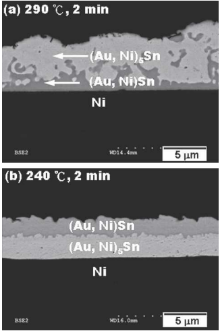
Figure 1. Microstructure of Sn/Au/Ni soldering (a) (Au, Ni) Sn near Ni side; (b) (Au, Ni) 5Sn near Ni side.
The metal compounds at the Cu substrate after soldering were mainly (Au, Cu) 5Sn and (Au, Cu) Sn (Figure. 2). It can be known that a small amount of Cu was incorporated into the sublattice of Au. Besides, the concentrations of Au and Cu in the (Au, Cu) 5Sn layer were different at varying temperatures. Low soldering temperature can lead to the decline of Cu content.
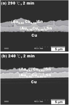
Figure 2. Microstructure of Sn/Au/Cu soldering.
Microstructure of solder joint after aging
Solder-Cu Interface
The microstructure evolution mechanism of Au80Sn20 solder joints is quite complex, and the law is difficult to determine and is very different from the SnAgCu and SnBiAg solder joints. For example, (Au, Cu) 5Sn and (Au, Cu) Sn have changed after bonding at 240 ℃ and aging at 240℃for 1 hour. (Au0.95, Cu0.05) 5Sn changed to (Au0.7, Cu0.3) 5Sn and (Au0.6, Cu0.4) 5Sn. (Au0.97, Cu0.03) Sn turned to discontinuous (Au0.94, Cu0.06) 5Sn, which indicates that the dissolution of Cu in solder increased significantly.
After aging at 240 ℃ for 10 hours, (Au0.94, Cu0.06), Sn did not change. However, Au-Cu-Sn with uncertain composition and Cu3Au appeared. Although the composition changes slightly, (Au, Cu) 5Sn always tended to grow next to the Cu layer.
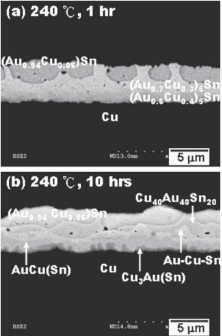
Figure 3. Microstructure of Cu interface after soldering and aging at 240℃.
Solder-Ni Interface
It can be found that the Ni interface still maintained a relatively complete structure after aging for 1000 hours, and the (Au, Ni) 5Sn layer remained continuous. However, (Au, Ni) Sn layer was replaced by the (Ni0.6, Au0.4) 3Sn2 and a thin Ni-Au-Sn layer with uncertain components. The appearance of (Ni0.6, Au0.4) 3Sn2 next to the Ni layer indicates that there was a certain amount of Au dissolved.
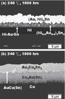
Figure 4. Comparison of microstructure of Ni interface and Cu interface after soldering and aging at 240℃.
Customers can contact Shenzhen Fitech if looking for high-temperature lead-free solder paste products. Fitech has advanced technology to produce gold-tin solder paste that can satisfy high-temperature lead-free soldering requirements.
Reference
Tsai, J.Y., Chang, C.W., Ho, C.E., Lin, Y.L. & Kao, C.R. (2006). “Microstructure Evolution of Gold-Tin Eutectic Solder on Cu and Ni Substrates”, Journal of Electronic Materials, vol.35(1).




 Back to list


