The Impacts of Voids on LED Package_Shenzhen Fitech

The Impacts of Voids on LED Package_Shenzhen Fitech
Display devices such as televisions and computers in daily life have become necessities for every household. The production of display products is inseparable from LED packaging technology. In order to achieve better display levels, it is necessary to significantly increase the number of light beads on LED displays. For the display screen to accommodate more LED chips, the chip size must be further reduced. To achieve this, a flip-chip LED (FC LED) will be applied. Moreover, FC LED can realize smaller thermal resistance and higher light efficiency.
For FC LED, eutectic gold-tin solder is commonly used, but the damage to chips caused by high soldering temperatures is obvious. SAC solder paste can also be used as a reflow soldering material for FC LED, and its soldering temperature is lower compared to gold-tin solder. The soldering process is shown in the following figure.

Figure 1. FC LED soldering process.
The reflow process will inevitably cause voids in the solder joints, which will harm the strength of the solder joints. In order to understand the factors that affect the formation of voids and the impact of voids during FC LED soldering, Liu et al. used a die bonder to place the LED chips onto the SAC305 solder paste with different thicknesses on OSP pads. The voids and strength of the solder joints after reflow were measured.
2. Test results
2.1 Void formation mechanism
In general, there are two basic mechanisms for the formation of voids. First, the flux solvent volatilizes during soldering. Some voids can escape from the molten solder, while the rest of the vapors that fail to escape will produce voids in the solder joints. Secondly, chips are usually picked and placed on the pads. When the solder paste volume is insufficient, voids will appear in the solder joints.
2.2 FC LED voids
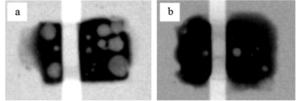
The figure below shows the void ratio of LED solder joints caused by different thicknesses of solder paste. When the SAC305 layer thicknesses were 20μm and 30μm, the percentage of voids in the solder joints was 46% and 3%, respectively. The solder volume significantly influences the void formation. As the volume of the solder paste increases, there are no large-scale voids in the solder joints, indicating that the solder paste can uniformly contact the LED chip during the chip placement process.

Figure 2. Voids of FC LEDs corresponding to different SAC305 thicknesses. a: Thickness=20μm. b: Thickness=30μm.
2.3 LED shear strength
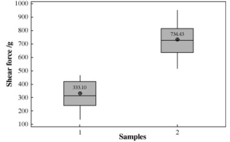
The presence of voids can affect the formation of IMC and reduce the connection area between chips and pads, which can weaken bonding. Therefore, when the void ratio in the solder layer decreases, the shear strength of LED packaging will increase. In addition, the stress applied to the solder joints will be concentrated near the voids and gradually lead to cracks.

Figure 3. Shear force of FC LEDs. 1: Solder thickness=20μm. 2: Solder thickness=30μm.
2.4 LED thermal performance
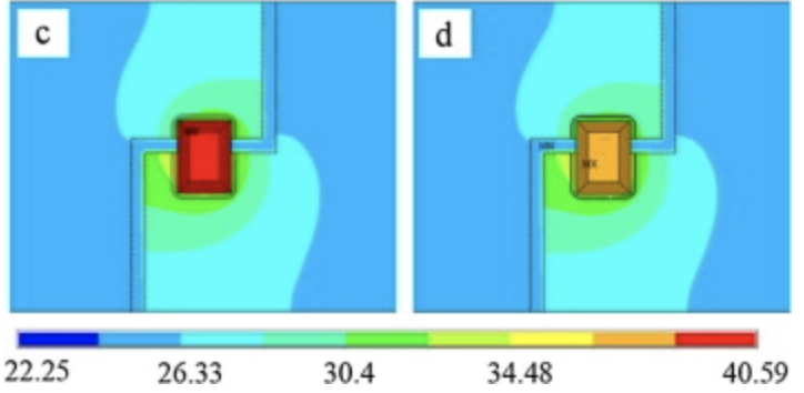
The thermal distribution of the chip under power can be detected through the infrared test. At a current of 100 mA, for LED chips with smaller solder thickness (higher void ratio), the surface temperature of the chip will be higher. Although an increase in solder thickness theoretically hinders heat conduction and increases chip temperature, the influence of voids dominates the thermal distribution under these testing conditions.

Figure 3. Surface temperature of FC LEDs. c: Solder thickness=20μm. D: Solder thickness=30μm.
3. Fitech's solder paste
Shenzhen Fitech can provide customers with high-quality SAC305 solder pastes (T6 and above). Fitech’s SAC305 solder pastes have stable viscosity, excellent wettability, and high bonding strength. Welcome customers who require solder materials to contact us.
4. Reference
Liu, Y., Leung, S.Y.Y., Zhao, J., Wong, C.K.Y., Yuan, C.A., Zhang, G.Q., Sun, F.L. & Luo L.L. (2014). Thermal and mechanical effects of voids within flip chip soldering in LED packages. Microelectronics Reliability, pp.2028-2033.
1. Soldering process
Sn42Bi58 s


 Back to list


