Introduction to the PCB Immersion Deposition Tin-Shenzhen Fitech

Introduction to the PCB Immersion Deposition Tin
The Immersion Deposition Tin process is a plating-free process for depositing tin on copper surfaces. It works by using copper and tin in an acid solution where the active tin is higher than copper, so that the pad copper foil reacts with the tin ions in the sink and the tin is oxidised and a uniform layer of tin is formed.
Displacement reaction equation for the Immersion Deposition Tin process
Cu(s)+ Sn2+(aq)→ Cu2+(aq)+ Sn(s)
Where Cu stands for copper, Sn for tin, s for solid and aq for aqueous solution. In the reaction, the ions of copper are replaced by those of tin, forming a solid layer of tin.
Comparison with tin spraying (hot air levelling) process:
The spray tin process involves spraying molten tin powder onto the surface of the substrate through a high pressure nozzle. The thickness and uniformity of the tin layer is not as good as the sink tin process and therefore may be less suitable for applications where high solder reliability is required.
The Immersion Deposition Tin process is relatively simple in composition, does not require a power supply or slot holder, and is easy, inexpensive and environmentally friendly to operate; and the Immersion Deposition Tin process can form a uniform film on the surface of the substrate and is therefore more suitable for closely spaced and micro-porous PCBs.
The main steps in the Immersion Deposition Tin process:
1. Cleaning: Before entering the plating solution, the substrate must be cleaned to remove oil, oxides and impurities.
2. Activation: The substrate is activated with an acidic solution to give the copper surface a good hydrophilic and catalytic character.
3. Immersion: Immerse the substrate in a plating solution containing tin ions and complexing agents, so that the tin ions react with the copper surface to form a uniform layer of tin.
4. Post-treatment: The residual plating solution is removed by rinsing with water, dried with hot air and the tin layer is passivated with organic substances to improve its corrosion and oxidation resistance.

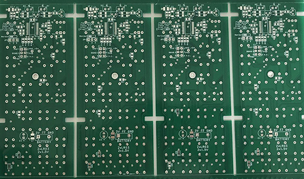
Figure 1: Chemically sunken tin plate
The Immersion Deposition Tin process has the following advantages:
1. The tin layer has good solderability, mountability and storability. The quality of the tin layer determines the performance and reliability of the PCB, and the Immersion Deposition Tin process ensures the quality of the tin layer, making the soldering and mounting process of the PCB easier and more reliable.
2. The absence of an interlayer between the tin layer and the copper layer prevents diffusion and dislodgement between the metals. The existence of an intermediate layer can lead to interaction between the tin and copper layers, affecting the performance and reliability of the PCB, while the Immersion Deposition Tin process can avoid such problems.
3. The process is simple, cost effective and environmentally friendly.
The Immersion Deposition Tin process also has some disadvantages:
1. The thickness of the tin layer is limited. As the original inactive copper replaced the more active tin particles, while the organic acid composition of the sink tin bath at a temperature of more than 70 degrees on the PCB group solder layer attacked violently, the solder resist layer and thus discolouration, dissolution, pollution of the bath. The industry generally requires sink tin layer thickness 0.8 ~ 1.2μm.
2. The tin layer is prone to tin whiskers. This can affect the reliability and performance of the PCB as a result of the uneven deposition rate of tin ions during the deposition process.
In short, the Immersion Deposition Tin process is a simple, low-cost, environmentally friendly surface treatment process to ensure the quality of the tin layer and the reliability of the PCB, has become one of the commonly used surface treatment processes in PCB production.


 Back to list


