μBGA, CSP in the Reflow Soldering of the Reasons for the High Rate of Cold Soldering_Shenzhen Fitech

μBGA, CSP in the Reflow Soldering of the Reasons for the High Rate of Cold Soldering
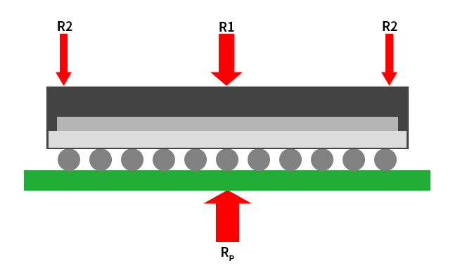
In the reflow soldering process, for μBGA and CSP packaged chips with dense feet (pitch ≤ 0.5mm), there is a risk of higher incidence of cold soldering due to the hidden nature of the soldering site and the difficulty of heat transfer to the solder ball solder joint site. Under the same peak temperature and reflow time conditions, the heat gained by the μBGA, CSP solder ball solder joints is significantly insufficient compared to other components with good solder joint exposure in hot air. This makes it difficult for the temperature of some μBGA, CSP bottom solder balls to reach the wetting temperature, which leads to the cold soldering problem.

Figure 1. CSP (chip-scale packaging) reflow soldering heat transfer pathway
Cold soldering is a phenomenon caused by the fact that the minimum required wetting temperature between the solder and the base metal is not reached during soldering, or localised wetting occurs, but the metallurgical reaction is incomplete. Cold soldering can lead to a degradation of the quality of the solder joint, which in turn affects the reliability and performance of the component.
So, how to reduce the cold soldering rate of μBGA, CSP in hot air reflow soldering? According to the reasons for cold soldering, improvements can be made in the following aspects:
Improve the reflow soldering heat supply, such as the use of "infrared + forced convection" heating. The use of infrared as the main heating source to achieve optimal heat transfer, and to capture the balanced characteristics of convection in order to reduce the temperature gap between the components and the PCB.
The structure of the package has a significant impact on the heating of the solder balls at the bottom of μBGA and CSP. Generally speaking, the thinner and smaller the package body, the smaller the obstruction to solder ball heating. Therefore, the heating efficiency of the solder ball can be improved by reducing the thickness and area of the package body. Alternatively, a metal layer or other thermally conductive material can be added to the interior of the package body to enhance the thermal conductivity of the interior of the package body.
The solder ball is a key part of the connection between μBGA, CSP and PCB, and its material and diameter have a direct impact on the cold soldering problem. Generally speaking, the material of the solder ball should match the pad material on the PCB to ensure good wetting performance. The diameter of the solder ball should be reasonably selected according to the degree of encapsulation and the size of the pads on the PCB, in order to avoid defective solder joints caused by too large or too small. In addition, the surface of the solder ball should be kept clean and smooth to reduce the effect of oxidation and pollution.


 Back to list


