Pin Device Desoldering Causes and Countermeasures_Shenzhen Fitech

Pin Device Desoldering Causes and Countermeasures
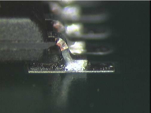
Desoldering refers to the reflow soldering process, one or more pins of the component can not be normal contact with the pad, resulting in incomplete or missing solder joints. Desoldering not only affects the performance and reliability of the circuit, but also increases the cost and difficulty of maintenance.

Component pin deformation: components in the production, transportation or storage process, may be subject to mechanical shock or vibration, resulting in pin deformation or fracture, thereby affecting the alignment and contact with the pad. In addition, the component's pin material, shape and size will also affect its thermal expansion coefficient and stress distribution with the pad, which in turn affects the formation and stability of the solder joint.
PCB pad coplanarity is poor: PCB is the carrier of components, the flatness and finish of its surface directly affects the components and pad fit and wettability. If the surface of the PCB has scratches, bumps, oil and other defects, or PCB thickness, material and number of layers do not match, will lead to poor coplanarity of the PCB, resulting in gaps or misalignments between components and pads, resulting in desoldering.
PCB warpage: PCB may be bowed or twisted deformed during fabrication, storage or reflow soldering due to temperature change, humidity change, mechanical stress or chemical reaction. This deformation can lead to relative displacement and stress concentration between the PCB and components, thus destroying the solder joints that have been formed or preventing the formation of new solder joints.
Components in the transmission process to be careful not to collide;
Avoid placing components in a pile;
Pay attention to the coplanarity requirements of PCB pads;
The bowing and twisting of the PCB should be less than 0.75%;
Cleaning and inspecting the PCB and components before and after reflow soldering to remove impurities and defects.


 Back to list


