Introduction to FCCSP Flip Chip Packaging Process_Shenzhen Fitech

Introduction to FCCSP Flip Chip Packaging Process
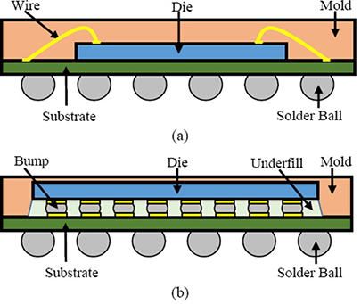
As mobile, networking and consumer electronic devices are updated, electronics are becoming more and more functional and smaller in size, with ever-increasing performance requirements for semiconductor packages. How to achieve higher and faster data transfer in thinner and smaller form factors has become a key challenge. As mobile devices require an ever-increasing number of inputs/outputs (I/Os) in a package, packaging solutions are migrating from traditional wire bonding packages to flip chip interconnects to meet these requirements. Flip chip packaging (FCCSP) is considered an effective solution for complex and highly integrated systems with multiple functions and heterogeneous mobile applications. As shown in Figure 1, semiconductor package interconnect technologies include lead bonding and flip chip bonding technologies.

Fig. 1. Schematic structure of (a) Wire Bonding Chip Scale Package (WBCSP), (b) Flip Chip Chip Scale Package (FCCSP).
FCCSP packaging is an advanced packaging technology that uses Flip Chip as an interconnection method to connect the chip directly to a laminate or moulded substrate, and interconnect the substrate electrodes through solder joints. Flip Chip bonding technology can connect more I/Os than wire bonding technology because it can utilise the front surface of the chip, and has the advantage of fast signal processing because the chip length is about 10 times shorter than the wire length. As a result, flip chip bonding technology is being used in various ways to interconnect high-density packages or digital packages that require fast signal processing.
1. FCCSP package can provide higher wiring density, lower inductance, and shorter signal path, thus optimising electrical performance for both low and high frequency applications.
2. Smaller package size, thinner package thickness, and lighter package weight to meet the demand for thin, light, small, and high density products.
3. Different bump options, such as copper post, lead-free solder, eutectic, etc., are used to adapt to different chip and substrate materials, improving reliability and compatibility.
4. Supports multi-chip (side-by-side stacking) applications for higher integration and functionality.
5. Supports in-package antenna (AiP) applications, utilising bottom-side chip placement (POSSUM™) technology to achieve higher signal quality and efficiency.
FCCSP packaging has been widely used in mobile devices (e.g. smartphones, tablets, etc.), automotive electronics (e.g. infotainment, ADAS, etc.), consumer electronics (e.g. digital cameras, game consoles, etc.), communication devices (e.g. baseband, RF, etc.), and artificial intelligence (e.g. AI chips, neural networks, etc.), etc., and it is a high-performance, highly-reliable, highly-flexible packaging solution.
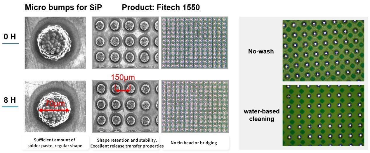
Fitech is currently the world's only manufacturer of full-size T2-T10 ultra-fine alloy solder powder electronic grade packaging materials, the production of tin powder and solder paste products with good viscosity stability, shape retention and stability and excellent release transfer performance, long time printing without tin beads, bridging defects, suitable for FCCSP, WBCSP and SiP and other packaging processes. Welcome to call us for more information.


 Back to list


