Solder Paste for SiP: Scales and Dimensions of Integration
Solder Paste for SiP: Scales and Dimensions of Integration
Solder Paste and Ultra-Fine Solder Manufacturer-Shenzhen Fitech is a comprehensive solder paste supplier integrating production, sales, research, and service of solder paste, epoxy solder paste, and solder powder. Fitech is the leading unit for the formulation of solder powder standards of the Ministry of Industry and Information Technology. Fitech's products include ultra-fine lead-free printing solder paste, ultra-fine lead-free dispensing solder paste, ultra-fine lead-free jetting solder paste, ultra-fine lead-free pin transfer solder paste, no-clean solder paste, water-soluble solder paste, high-temperature solder paste, medium-temperature solder paste, low-temperature solder paste, etc. Fitech can manufacture electronic-grade packaging solder powders with particle sizes from T2-T10.

Introduction
Integration refers to the process of combining different units to achieve specific functions. Integration refers to human activities rather than natural processes. Integrated circuits and system integration are relatively common terms. In this article, we dissect modern electronic integration technology from the aspects of scale and dimension.
Integration
Integration Scales
Scale is generally understood as the length measurement. Specified limits can be extended to standards and law. In this context, scale refers to the size of the object being described. This article will analyze the scale of integration from small to large. Let's start with the smallest elementary particles.
Elementary Particles
The world consists of 61 elementary particles.
The elementary particles are divided into three categories: quarks, leptons, and bosons.
Only electrons, photons, and neutrinos are the particles that exist stably in nature and can act in the macroscopic world. The famous quarks are trapped in composite particles such as protons and neutrons and cannot be released.
Electrons (leptons): Electron is the most well-understood and widely used elementary particle. Today, modern technology basically revolves around electronics, without which technology development would be at a standstill.
Photons (bosons): The application of photons is earlier than that of electrons. It has been used since ancient times, and photons are inseparable from daily life to the latest scientific fields.
Neutrinos (leptons): Neutrinos are very difficult to detect, so they are called mysterious particles. Although neutrinos are not widely used at present, they have great potential, have a speed close to the light, and can pass through all objects without hindrance. Neutrinos can be used in neutrino communication, stratigraphic scanning, and other fields in the future.
Those elementary particles that cannot exist independently in nature cannot directly interact with the macroscopic world, so they cannot be practical. Their impact on human beings is far less than electrons, photons, and neutrinos.
Atoms
Now lets scale up to atoms.
There are 118 elements currently known to humans, ninety-two of which are from nature, and the rest are artificially synthesized. The smallest unit that represents an element is called an atom. Different atoms make up different substances.
An atom consists of a nucleus and electrons orbiting the nucleus. The nucleus occupies only one hundred billionths of the volume of the atom. Hence, the atom volume is determined by the electrons outside the nucleus.
The electron has wave-particle duality. It does not have a definite orbit like the motion of macroscopic objects. It is impossible to predict where it will appear in the extra-nuclear space at a certain moment. It looks like a negatively charged cloud surrounding the nucleus named an electron cloud.

Take the most commonly-used silicon element in semiconductors as an example. There are 14 electrons outside the silicon nucleus. The first layer has 2 electrons, the second layer has 8 electrons, and the outermost 4 electrons are valence electrons.
There are no obvious free electrons in the silicon crystal. The four electrons in the outermost layer of the silicon atom are neither as active as in the conductor nor as tightly bound as in the insulator. Silicon activity is between the conductor and the insulator, causing semiconductor properties. Silicon conducts electricity but is not as conductive as metals and increases with temperature.
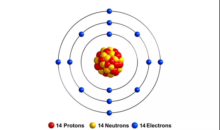
The scale of an atom. An atom does not have a precisely defined outermost layer. The defined atomic radius is measured from the average internuclear spacing of adjacent atoms. What exactly is the distance between silicon atoms in a silicon crystal?
The most basic geometric unit that constitutes a crystal is called a unit cell. A silicon crystal is a face cube with a side length of 0.543nm. Take one face of the silicon atomic unit cell as a plane, the silicon atom arrangement is shown in the figure below. The minimum spacing of silicon atoms in this plane is 0.384 nm, and the arrangement width of three silicon atoms is 1.152 nm.
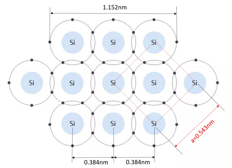
So, how many silicon atoms are in one cubic nanometer?
In the unit cell of a face-centered cube composed of silicon atoms, each of the eight vertices and six faces has a silicon atom. There are also four silicon atoms located at one-fourth of the four space diagonals, respectively. The number of atoms in each silicon unit cell is 8 (8 × 1/8 + 6 × 1/2 + 4 = 8).
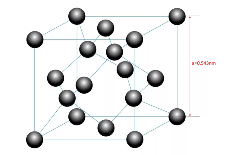
The unit cell edge length of silicon is represented by a (lattice constant). At 300K, a is equal to 5.4305Å (0.543nm).
8 ÷ (0.543³)=49.97≈50. Therefore, the number of silicon atoms in 1nm³ is 50. The same result will be obtained by calculating the density of silicon material and the mass of silicon atoms.
In order to improve the conductivity of silicon, a small amount of 5-valent element is doped to form an N-type semiconductor, or a small amount of 3-valent element is doped to form a P-type semiconductor.
No matter what kind of element is added, the lattice structure of silicon will basically not be changed. Therefore, the distance between atoms will not change, and the number in 1nm³ will remain the same, which is still 50.
At the nano-scale, atoms are still countable.
From Atoms to Function Cells
What is a function cell? We define it as the smallest unit of function. In integrated circuits, transistors can be defined as functional cells. Apparently, resistors, capacitors, inductors, diodes are also function cells.
Function cells are composed of atoms, and the functions is realized by controlling electrons. Another explanation is that the functions of cells are endowed by electrons. If they can reasonably control electrons, they have corresponding functions.
The realization of the function comes from the needs of reality, human wisdom, and those great inventions and discoveries.
Let's take the most typical functional cell transistor in an integrated circuit as an example.
The reason why transistors can be functional cells is that they can effectively control electrons.
The figure below is the current mainstream FinFET transistor. By applying a reasonable voltage to the gate, electrons can flow from the source to the drain, thereby generating current.
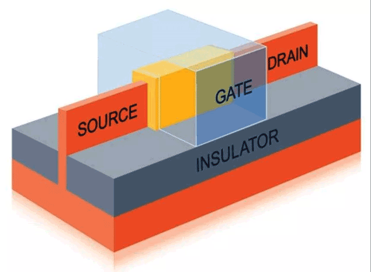
Through the on and off of transistors, different states can be represented. Multiple transistors can be combined to form different logic circuits to complete various functions.
As long as it can perform the same function, the small volume of function cells will be more welcomed. How small can function cells be?
The existing silicon-based transistors is roughly restricted by two factors. One is the minimum structure width in the transistors, and the other is the area (volume) occupied by the transistors.
We know from the analysis that the width of three silicon atoms arranged side by side exceeds 1nm. Can the minimum structural width of the transistor be even less than 1nm? It is not easy to conclude now. In addition to the difficulty of manufacturing with such a small width, the transistor operation is restricted according to the existing theory.
New types of transistors, such as single-atom transistors, have a minimum structural width of one atom. The control of the on and off of the transistors is through manipulating a single atom.
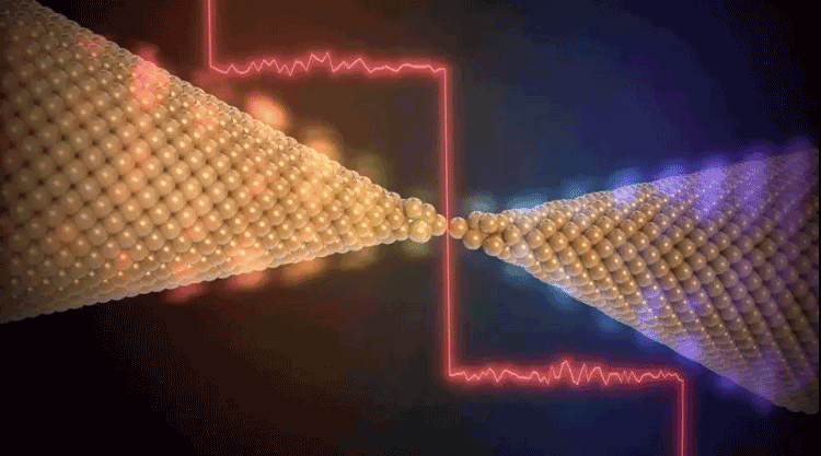
It is said that the energy consumption of a single-atom transistor will be only one ten-thousandth (1/10,000) of that of a silicon-based transistor, which is a decisive advantage for future applications.
From Function Cells to Common Systems
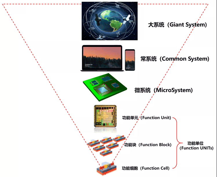
Function cells can be small, and current technology supports the integration of more than 10 billion transistors on a chip with a fingernail size. Multiple function cells can form a functional block, and then multiple function blocks form a function unit. The multiple function units eventually form a microsystem.
However, for human beings, the scale of products needs to be suitable for human needs and must be comparable to the scale of human beings.
For example, in mobile phones and computers, the phone needs to be frequently held in hands, so it needs to be equivalent to the size of the human hand. The laptop needs to be placed on the desk or knee, so it should be as large as the horizontal size of the human body.

This type of system is called a common system, which means that ordinary people can contact and use the system frequently. A common system consists of microsystems and functional units and is ultimately achieved by function cells.
Because the common system needs to match the scale of human beings, even if the technology is advanced, its scale will not change too much. However, in order to meet more functional needs of human beings, the function cells contained in the common system will continue to increase. Therefore, the function density will continue to increase.
Moreover, in the process of the development of human civilization, this trend will continue, which is also in line with the description of the Function Density Law.
 From Common Systems to Giant Systems
There is another type of system that serves people, but it is for groups rather than individuals. As a result, the system scale can be very large. Thus ,this system is called a giant system, including a manned spaceflight system, wireless communication network system, GPS global satellite positioning system, and so on.
Giant systems are usually very complex, generally composed of many common systems, micro-systems, or functional units.
For example, the GPS is divided into three parts. The space part consists of 24 satellites. The ground part consists of the main control station, the monitoring station, and the ground antenna, and the user equipment part is made up of various GPS signal receivers.
The GPS can perform real-time high-precision positioning speed measurement and precise timing for various mobile users such as ground vehicles, ships, aircraft, satellites, and spaceships.
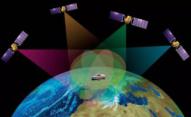
Like ordinary systems, in order to meet more functional requirements, the function density of giant systems will continue to increase, and this trend will continue with the development of human civilization, which is also corresponding to the description of the law of functional density.
Integration Scale Summary
Here, we summarize the scale of the ensemble with two graphs.
We divide the electronic system into six levels, which is called the 6-level classification method of an electronic system (see the book "Microsystem Based on SiP Technology" for details).
The function cell is the smallest function unit. The scale from small to large is function cell, function block, and function unit, which are three different function units, and thus constitute a microsystem, common system, and giant system just shown in the figure below.
Then, we analyze the function cells. The function cells can be divided into four levels according to the hierarchy. Basic particles form atoms, atoms form unit cells, and unit cells form function cells.
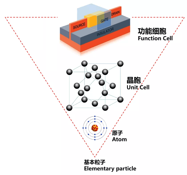
In this article, from elementary particles to the most complex systems that can be realized by humans, we divide them into 10 (4+6) levels according to the scale. Function cells are the most critical link, which is the basic unit and carrier of functions similar to human cells. It is the constituent unit of human life and the carrier of wisdom.
Each level or link requires different people to explore, realize, innovate, develop, and integrate human wisdom.

SAC Solder Paste SACS Solder Paste SnBiAg Solder Paste SnBiAgSb Solder Paste SnBiAgX Solder Paste SnBi Solder Paste BiX Solder Paste AuSn Solder Paste SnSb Solder Paste SnPb Solder Paste Anisotropic Conductive Paste Ultra-Fine-Pitch Flux

Integration
Integration Dimensions
The world that humans can perceive has only three spatial dimensions. Including time, the world is often referred to as the four-dimensional spacetime.
The 11-dimensional spacetime described in string theory cannot be proven to exist. Even if it exists, it is like those elementary particles that are imprisoned in the microscopic world and cannot be perceived in the macroscopic world. Therefore, it has almost no impact on human activities.

In our usual understanding, zero dimension is a point, one dimension is a line, two-dimension is a plane, and three-dimension is solid.
Integration is the process of bringing different units together and realizing their specific functions. Therefore, zero-dimensional points and one-dimensional lines are not suitable for integration. In reality, the main integration method is two-dimensional plane integration and Three-dimensional stereo integration.
In practical applications, it is really tough to classify integration only in two-dimension and three-dimension. For example, some people use "fake 3D" and "real 3D" to distinguish different types of chip stacking methods.
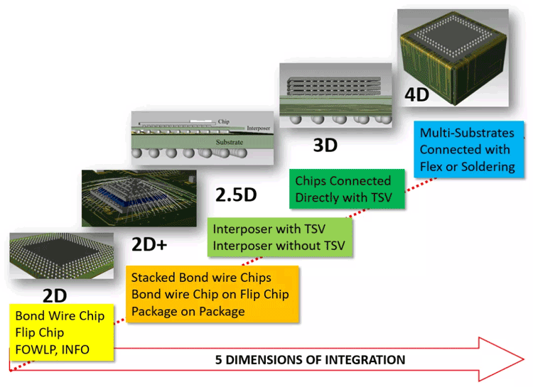
Let's discuss the integration with five dimensions, including 2D, 2D+, 2.5D, 3D, and 4D. The purpose is to facilitate the classification and distinction of integration and to be compatible with mainstream thoughts.
Furthermore, we provide two important criteria, which are physical structure and electrical interconnection.
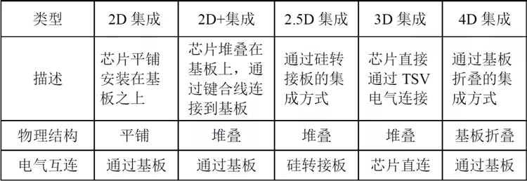
The integration described below is mainly for the field of integrated circuit packaging, and so on for other fields.
 2D Integration
2D integration refers to the integration of chips and passive components mounted horizontally on the surface of the substrates.
A coordinate system is created with the lower left corner of the upper surface of the substrate as the origin. The upper surface of the substrate is located in the XY plane, and the substrate is normal as the Z axis.
Physical structure: All chips and passive devices are mounted on the substrate plane, the chips and passive devices are in direct contact with the XY plane, and the wiring and vias on the substrate are located below the XY plane; a few bond points are directly connected by bond wires).
The most common 2D integration techniques are used in MCMs, some SiPs, and PCBs.
MCM (Multi-Chip Module) is a high-density mounting of multiple bare chips on the same substrate to form a complete component.
In the traditional packaging field, all packaging serves the chip without the idea of integration, playing the role of chip protection, scaling up, and electrical connection. With the rise of MCMs, the concept of integration has emerged in packaging. Thus, packaging has undergone essential changes. MCMs change the concept of packaging from chips to modules, components, and systems.
The process route of 2D integrated SiP is very similar to that of MCMs. The main difference is that the scale of 2D integrated SiP is larger than that of MCMs, and it can form an independent system.

2D Integration Schematic Diagram
Furthermore, FOWLP-based integrations such as INFO, without a substrate, can also be attributed to 2D integration. At present, the arrangement of transistors in integrated circuits is basically a 2D integration.
2D integration is the easiest for EDA. The figure below shows the 2D integration design implemented in EDA.
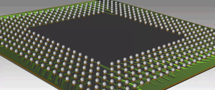
2D Integration Design by EDA
2D+ Integration
2D+ integration refers to the traditional stacking integration of chips connected by wires. Some people may think chip stacking is a 3d structure. Why should it be defined as 2D+ integration?
There are two reasons to explain. The first reason is that 3D integration currently refers to the integration through 3D TSV to a large extent. In order to avoid conceptual confusion, we define this traditional chip stacking as 2D + integration. The other reason is that although the physical structure is 3D, the electrical interconnection needs to pass through the substrate, which is firstly achieved by bonding the chips to the substrate through wires and then performing electrical interconnection on the substrate. This process is the same as 2D integration but realizes improvement of structural stacking over 2D integration, which can reduce packaging space. Therefore, it is called 2D+ integration.
Physical structure: All chips and passive devices are located above the XY plane, but some chips do not directly contact the substrate. The wiring and vias on the substrate are located below the XY plane. Electrical Interconnects: All chips need to go through the substrate (except for very few bonding points that are directly connected by wires)
Several integrations shown in the figure below belong to 2D+ integration.


2D+ Integration Schematic Diagrams
In addition, the integration method of PoP (Package on Package) can also be judged according to its physical structure and electrical connection, and it can be attributed to 2D+ integration.
EDA has always provided good support for 2D+ integration. The figure below shows the 2D+ integration design implemented in EDA.
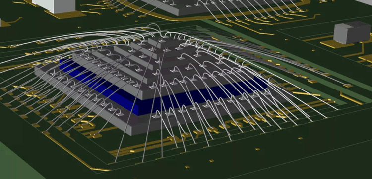
2D+Integration Design by EDA
 2.5D integration
2.5D, as the name suggests, is between 2D and 3D. It usually refers to a dimension that has both 2D characteristics and some 3D characteristics. In reality, there is no 2.5D.
Physical structure: All chips and passive components are above the XY plane, and at least some of the chips and passive components are mounted on the interposer. Above the XY plane, there are wiring and vias of the interposer. There are wiring and vias for the substrate below the XY plane. Electrical Interconnect: The interposer provides electrical connections to the chips on the interposer.
The key to 2.5D integration is the interposer. Generally, there are several situations. 1) Whether the interposer uses a silicon transition board; 2) Whether the interposer uses TSV; 3) The interposer uses other types of materials. On the interposer, we call the via that goes through the interposer TSV, and for the glass interposer, we call it TGV.
The integration of silicon interposer with TSV is the most common 2.5D integration technology. The chip is usually connected to the interposer through micro-bumps. The silicon substrate as the interposer is connected to the substrate by bumps. The surface of the silicon substrate undergoes a process of RDL, and TSV is used as the channel for the electrical connection between the upper and lower surfaces of the silicon substrate. This 2.5D integration is suitable for the case of relatively large chip scale and high pin density. The chip is generally installed on the silicon substrate through a flip chip.

Schematic Diagram of 2.5D Integration with TSV
The structure of 2.5D integration without TSV in the silicon interposer is shown in the figure below. There is a large bare chip directly mounted on the substrate. The connection between the chip and the substrate can be wire bonding or flip chip. Due to the large area above, several smaller bare chips can be installed, but the small chips cannot be directly connected to the substrate. Hence, an interposer needs to be inserted, and multiple bare chips are installed above the interposer, with RDL on the interposer. Wiring, the signal of the chip can be drawn out to the edge of the interposer and then connected to the substrate through Bond Wire. This type of interposer usually does not require TSV, which only needs to be electrically interconnected through wiring on the upper surface of the interposer, which uses wires to connect to the package substrate.

Schematic Diagram of 2.5D Integration without TSV
Now, EDA design tools have good support for 2.5D integration, and the figure below shows the 2.5D integration design implemented in EDA tools.
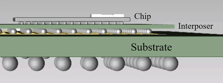
2.5D Integration Design by EDA
 3D Integration
The main difference between 3D and 2.5D integrations is that 2.5D integration is to perform wiring and TSV on the interposer, while 3D integration is to conduct TSV and RDL directly on the chips for the electrical connection between the upper and lower chips.
Physical structure: All chips and passive components are located above the XY plane, and the chips are stacked together. There are TSVs that pass through the chip above the XY plane, and the wiring and vias of the substrate are below the XY plane. Electrical Interconnection: Direct electrical connection of chips through TSV and RDL.
As shown in the figure below, 3D integration is mostly used in homogeneous chip stacking, in which identical chips are stacked vertically and interconnected by TSVs that pass through the chip stack. Similar chip integration is mostly used in memory integration, such as DRAM Stack, FLASH Stack, etc.

Schematic Diagram of 3D Integration with the Same Types of Chips
In the 3D integration of different types of chips, two different chips are generally stacked vertically and electrically connected by TSVs. The stacked chips are interconnected with the underlying substrate. Sometimes it is necessary to make RDLs on the surface of the chips to connect the upper and lower TSVs.

Schematic Diagram of 3D Integration with Different Types of Chips
In addition, the current 3D Nand Flash is to directly fabricate multi-layer memory cells on a chip, which is also a 3D integration technology.
Now, EDA has good support for 3D integration, and the figure below shows the 3D integration design implemented in EDA.
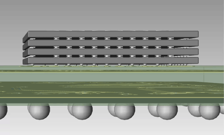
3D Integration Design by EDA
 4D Integration
2D, 2D+, 2.5D, and 3D integration were introduced earlier. How is 4D integration defined?
In the several integrations described above, all chips, interposers, and substrates in the three-dimensional coordinate system have Z-axis vertically upwards. All substrates and chips are installed in parallel. In 4D integration, the structure is different.
When the XY planes of different substrates are nonparallel, the Z-axis directions of different substrates are offset, which can be defined as 4D integration. Physical structure: Multiple substrates are installed in a nonparallel manner, and components are installed on each substrate. The installation methods of components are diversified. Electrical interconnection: The substrates are connected by flexible circuits or soldering. The electrical connections of the chips on the substrates are diversified.
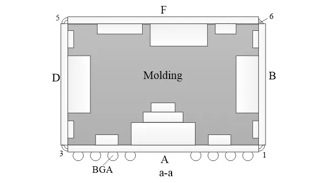
4D Integration Diagram
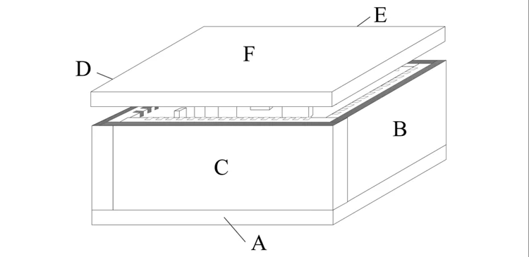
Schematic Diagram of 4D Integration with Air-Tight Ceramics
The definition of 4D integration is mainly about the orientation and interconnection of multiple substrates, so each substrate in 4D integration may include 2D, 2D+, 2.5D, and 3D integration methods.
The 4D integration technology can solve the problems that cannot be solved by parallel three-dimensional stacking, providing more and more flexible chip installation space, solving the heat dissipation problem of high-power chips, and handling the air tightness problem concerns in aerospace and other fields.
Now, the EDA also has good support for 4D integration. The figure below shows the 4D integration design implemented in the EDA.
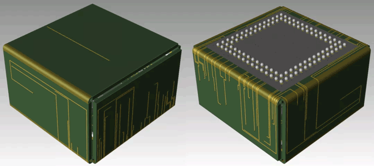
4D Integration Design by EDA
4D integration technology has improved the flexibility and diversification of integration. Looking forward to the future, 4D integration will surely occupy a place in various integration dimensions. It will become an important integration technology after 2D, 2D+, 2.5D, and 3D integration technologies.
In a strictly physical sense, based on the existing human cognition, all objects are three-dimensional. The two-way foil does not exist, and the four-dimensional space is more to be verified.
In order to distinguish different integration methods, we divide them into 2D, 2D+, 2.5D, 3D, and 4D.
Integration Dimension Summary
Here, we use a diagram to summarize the dimensions of integration. The following diagram contains the EDA design legend of 5 integration dimensions and the specific integration types included in each dimension.
Conclusion
Integration generally refers to human activities rather than natural processes. Therefore, integration is an important means to transform the world.
In this article, we analyze modern electronic integration technology from two aspects of scale and dimension, both of which belong to the category of space. One represents the size of the space, and the other represents the orientation.
The scale of integration ranges from the smallest elementary particles to the most complex giant systems, which is divided into ten levels for description. The dimension of integration defines five dimensions for classification and description.
From the spatial axis, our description of the integration is sufficient.
Later, I will write an article to analyze the integration from the time axis, which is divided into a short-time axis and a long-time axis. Readers are welcome to continue to pay attention, read, and make suggestions.
Source:SiP与先进封装技术


 Back to list


