Mini LED Packaging (SMD, IMD, COB, Wire Bonding, Flip-Chip)
Mini LED Packaging (SMD, IMD, COB, Wire Bonding, Flip-Chip)
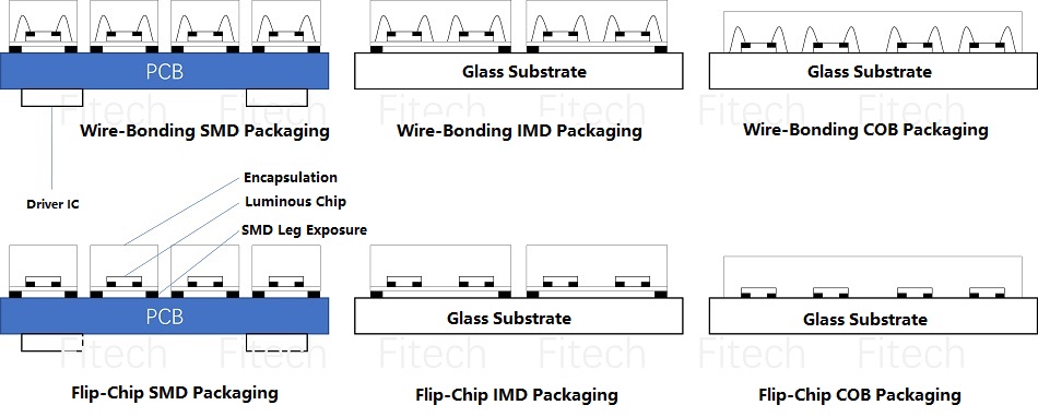
The purposes of LED packaging are protecting the chip and realizing the signal connection. In addition, it can stabilize the LED performance, improve luminous efficiency, and prolong the service life. The packaging process flow incluces die bond, soldering, sealing, baking, dicing, Binning, and packaging. LED packaging techniques include SMD, IMD, and COB. According to the packaging directions of the chip, packaging methods include wire bonding and flip-chip. Regarding the substrate material, packaging methods consist of PCB substrate packaging and glass substrate packaging. Flip-chip and COB have excellent heat dissipation, high reliability, and stronger protection to reduce maintenance costs. IMD is also popular because it has the advantages of easy binning, outstanding compatibility with the SMT process, convenient repair, etc.

As the chip size of mini LED has become smaller, the number of chips per unit area has increased sharply. Hence, the die-bonding devices must have high transfer efficiency in the packaging stage. The die bonding device is an important device in packaging, which is responsible for obtaining the wafer and mounting it on the PCB or glass substrate, followed by defect detection. Due to the increase in the number of mini LED chips per unit area, the transfer speed and precision of die-bonding devices determine the packaging yield. Packaging yield is the key to reducing costs and achieving mass production. Currently, the die bond transfer includes the pick-and-place scheme, the thorn scheme, and the laser transfer scheme. Pick-and-place is the mainstream technology with high maturity and cost-effectiveness.
In addition, the standard technical path of test and repair has not yet been formed. Mini LEDs need to complete the photoelectric test before delivery and finish the colorimetric parameter test and repair to ensure the yield of the final product. There are many kinds of devices in this field. It is tough to test and repair massive numbers of micron-sized lamp beads. As a result, a standardized technical path has not yet been realized.


 Back to list


