The Mainstream Lead-Free Soldering Practices
The Mainstream Lead-Free Soldering Practices
Shenzhen Fitech——Research Center——Jianwen Yu
Abstract
Lead not only pollutes water but also damages soil and air. Tin-lead alloy solder (Sn/Pb) used in electronic manufacturing is one of the main sources of pollution to the environment. Therefore, the application of lead-free soldering technology is an inevitable trend. It is imperative to realize comprehensive lead-free electronic manufacturing to reduce environmental pollution and meet the demand for green electronic products in domestic and foreign markets. This article will introduce lead-free alloys and PCB surface finishes.
1.Lead-Free Alloys
At present, lead-free solders include SnCu (doped with Ni, Co, Ce) and SnAg (+Cu, +Bi, +Sb, +dopants, such as Mn, Ti, Al, Ni, Zn, Co, Pt, P, Ce), SnZn (+Bi). The most popular lead-free alloys are SnAgCu with 1%-5% Ag, and SnBi (+Ag) (melting point 140°C) is also becoming popular.
Adding Ni to Sn-0.7Cu can reduce copper corrosion and stainless steel corrosion. 304 stainless steel corrosion rate: SAC305 > Sn-0.7Cu > Sn-0.7Cu-0.05Ni; Copper corrosion rate SAC305 > Sn63 > Sn-0.7Cu-0.05Ni[1]. In drop test, dopant additions such as Mn, Ti, Ce, Bi can enhance impact resistance. SAC105+0.05Mn/Ce≈SnPb >105 >305. After thermal cycling, impact resistance of SAC105+Ce is better than that of SAC105+Mn, followed by 305, 105 and SnPb[2].
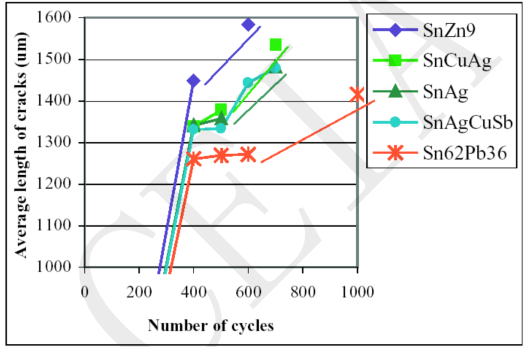
As shown in the figure below, as the number of thermal cycles increases, lead-free alloy cracks are longer than that of SnPb36Ag2. The cracks of SnAg3.5, SnAg3.8Cu0.7 and SnAg2.6Cu0.8Sb0.5 have no obvious difference. SnZn9 has the longest cracks[3].
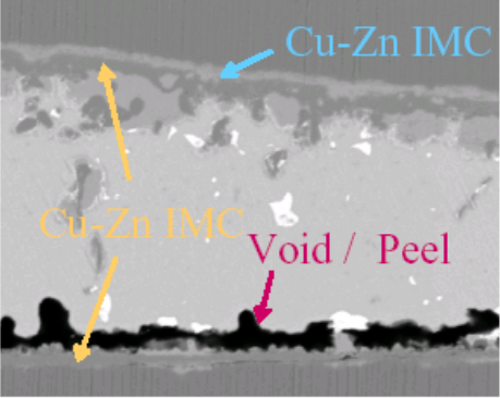
Strength loss of 89Sn-8Zn3Bi solder joints is caused by the growth of IMC layer and the formation of voids[4].
2.The Mainstream Lead-Free PCB Surface Finishes
Lead-free PCB surface finishes mainly include OSP, Ni/Au plating (ENIG), Ag plating, Bi plating, Pd plating, Ni/Pd plating, Ni/Pd/Au plating (ENEPIG), Ni/Pd(X) plating, and Sn plating (SnAg, SnBi, SnCu, SnNi).
2.1 OSP
OSP is to chemically grow an organic film on the clean bare copper surface. Because OSP is organic, it is cheaper than the tin jetting process.
The only function of this organic film is to prevent the inner copper foil from oxidization before soldering. As soon as it is heated during soldering, the film volatilizes. Solders can connect copper wires and components. However, this layer of the organic film is not resistant to corrosion. An OSP-treated circuit board cannot be soldered after being exposed to the air for more than 10 days.
2.1.1 Pros and Cons of OSP
Pros: It has all the advantages of bare copper board soldering. The expired board can undergo surface finish again.
Cons: OSP is transparent, so it is difficult to distinguish whether the board has been treated by OSP. OSP is insulating and non-conductive, which will affect electrical testing. Therefore, the test point must be printed with solder paste through a stencil to remove the original OSP layer in order to contact the pinpoint for electrical testing. OSP cannot be used for handling electrical contact, such as keyboard surfaces. OSP is susceptible to acid and temperature effects. When undergoing secondary reflow soldering, soldering needs to complete within a certain period of time. Usually, the effect of the second reflow soldering will be poor. If the storage time exceeds three months, the boards must conduct surface finish again. Boards should be used up within 24 hours after opening the package.
2.1.2 OSP Mechanism
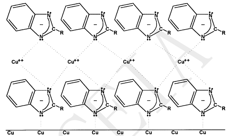
As shown in the figure below, the addition of benzimidazole coating on the copper surface for OSP can reduce the oxidation of the board surface[5].
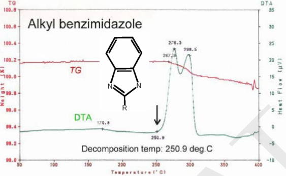
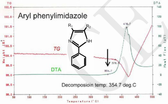
The following figures are the TG-DTA curves of the organic molecules of the mainstream OSP surface coating and the organic molecules of the new-style OSP surface coating. The decomposition temperature of the new one is 100°C higher than the original[6].
2.2 Electroless Nickel/Immersion Gold(ENIG)
ENIG is to chemically form a thick nickel-gold alloy layer on the copper surface with excellent electrical properties, which can protect the PCB for a long time. The deposition thickness of the inner nickel layer is generally 3-6 μm. The deposition thickness of the outer gold layer is 0.05-0.1 μm. OSP acts as a rust barrier, while ENIG can be useful to achieve excellent electrical performance during long-term use of the PCB. In addition, ENIG also has better environmental tolerance than other surface finishes.
2.2.1 ENIG Mechanism
(1)Ni Plating
3NaH2PO2+3H2O+NiSO4→3NaH2PO3+H2SO4+H2+Ni0 or
Ni+++H2PO2-+H2O→Ni0+H2PO3-+2H+
2R2NH·BH3+3Ni+++2H2O→NiB+2Ni+2R2NH+HBO2+6H++3/2H2
(2)P deposition
2H2PO2-+Hads→H2PO3-+H2O+OH-+P
3H2PO2-→H2PO3-+H2O+2OH-+2P
(3)Immersion Gold
Ni0+2Au+→Ni+++2Au0
Ni+2Au(CN)2-→Ni+++2Au+4CN-
2.2.2 Pros and Cons of ENIG
Pros: The PCB treated by the ENIG method is flat and has outstanding coplanarity, which is suitable for the contact surface of keys. ENIG has excellent solderability. Gold will quickly melt into the molten solder, and the solder and Ni form a Ni/Sn metal compound.
Cons: The process is complex. It is necessary to control the process parameters strictly for good results. The most troublesome thing is that EING-treated PCB surfaces are prone to generate the black pad effect during the ENIG or soldering process. The direct manifestation of the black pad is excessive oxidation of Ni and high gold contents. The solder joints become brittle and less reliable.
2.3 Electroless Nickel Electroless Palladium Immersion Gold (ENEPIG)
ENEPIG produces a palladium layer between the nickel and gold. In the deposition reaction of the replacement of gold, the electroless palladium layer will protect the nickel layer from excessive corrosion by the gold. The palladium prevents the corrosion caused by the replacement reaction and make full preparations for immersion gold. The deposition thickness of nickel, palladium and gold are 3-6 μm, 0.1-0.5 μm, and 0.02-0.1 μm, respectively.
2.3.1 Electroless Palladium Mechanism
Pd2++NaH2PO2+H2O→PdO+NaH2PO3+2H+
3NaH2PO2→2P+NaH2PO3+2NaOH+H2
2.3.2 Pros and Cons of ENEPIG
Pros: ENEPIG prevents the occurrence of “black nickel” because there is no replacement of gold to attack the surface of nickel to cause grain boundary corrosion. Electroless palladium performs like a barrier layer to eliminate copper migration to the gold layer, preventing solderability decline. The electroless palladium layer completely dissolves in the solder. There is no high-phosphorous layer on the alloy interface. Meanwhile, when the electroless palladium dissolves, a new electroless nickel layer is exposed to generate an effective nickel-tin alloy to withstand multiple lead-free reflow cycles. Besides, it has excellent bonding with gold wire, which is Ideal for the components such as SSOP, TSOP, QFP, TQFP, PBGA, etc.
Cons: ENEPIG is not widely used because palladium is scarce and expensive. The process control requirements are as strict as ENIG.
Fitech has been focusing on microelectronics and semiconductor packaging solder for more than 20 years. Fitech is a world-leading packaging material and solution provider for microelectronics and semiconductors. It is a national high-tech enterprise deeply engaged in microelectronics and semiconductor packaging materials. It is the only electronic-grade packaging material manufacturer in the world that can manufacture T2-T10 ultra-fine solder powder. Fitech's solder paste, epoxy solder paste, and alloy solder powder are widely used in microelectronics and semiconductor packaging. The global SMT electronic chemical manufacturers, micro photoelectric manufacturers, and semiconductor packaging testers have recognized the products. However, the problems with microelectronics and semiconductor packaging materials are extensive. We only describe the common problems here. The issues involved may be different because of different technological processes. Welcome to communicate and discuss the specific question with our professionals. We hope to keep pace with the times with our partners and explore new problems, technologies, and complex processes together. Fitech strives to provide partners with professional and thoughtful microelectronics and semiconductor packaging and soldering materials services.
Reference
[1]. Keith Sweatman, Shoichi Suenaga, Masaaki Yoshimura and Tetsuro Nishimura (Nihon Superior), Masahiko Ikeda (Kansai University), “Erosion 5 of Copper and Stainless Steels by Lead-Free-Solders”, Apex, S27-4, Anaheim, CA, Feb, 2004.
[2]. Liu etc, SMTAI, p.920-934, October 4-8, 2009, San Diego, CA.
[3]. Günter Grossmann, Giovanni Nicoletti, Ursin Solèr , “Results of Comparative Reliability Tests on Lead-free Solder Alloys”, 52nd ECTC, S30-P1, San Diego, CA, May 28-31, 2002.
[4]. Hirokazu Tanaka, Yuuichi Aoki, Makoto Kitagawa and Yoshiki Saito (ESPEC CORP.), “Reliability Testing and Failure Analysis of Lead-Free 8 Solder Joints under Thermo-Mechanical Stress”, Apex, S28-1, Anaheim, CA, Feb, 2004.
[5]. Joseph D. DeBiase, “Organic Solderability Preservatives: Benzotriazoles and Substituted Benzimidazoles”, SMI 96, San Jose, CA, September 10-12, 1996.
[6]. Koji Saeki, (Shikoku Chemicals Corporation) and Michael Carano,
(Electrochemicals, Inc.), “Next Generation Organic Solderability Preservatives (OSP) for Lead-free soldering and Mixed Metal Finish PWB’s and BGA Substrates”, Apex, S10-2, Anaheim, CA, Feb, 2004.




 Back to list


