Achieving High Reliability Lead-Free Solder Joints through Surface Finishes
Achieving High reliability Lead-Free Solder Joints through Surface Finishes
Fitech——Research Center——Shuquan Luo
Abstract
With the continuous development of semiconductor technology, the miniaturization, high speed, and high reliability of electronic packaging have raised higher requirements for the refined process in the electronic packaging process. The surface finishes refer to the physical or chemical treatment of different soldered substrates obtaining high-reliability solder joints.
Electroless plating is a process in which metal ions continuously deposit on the metal surface with a redox reaction assisted by the catalysis of the metal surface. Electroless plating must be carried out on the surface of materials with autocatalytic properties. Therefore, electroless plating is also called autocatalytic plating. The chemical plating techniques includes nickel plating, gold plating, copper plating, cobalt plating, etc. After different chemical plating, a protective plating layer is formed on the soldering substrate, which plays a positive role in high-reliability solder joint formation during the soldering process. Chemical plating is popular in the field of electronic packaging.
1. The issues of Immersion Tin
1.1 Immersion tin requires a long process time
Tin plating is putting the substrate into a metal salt solution. The metal deposits on the substrate to form a layer according to the principle of chemical replacement, achieving the desired soldering effect.
The immersion tin process generally requires 10 to 15 minutes to finish because of the process complexity. If using OSP, the processing time is much shorter, which only costs 1 minute. The immersion silver process time is also relatively short, requiring 0.5 to 3 minutes.
1.2 The accumulation of copper during tin plating raises the analysis of tin layer thickness and cost
During immersion tin, Sn2+ is replaced by Cu2+ using thiourea chemistry. Every single tin atom precipitation leads to two Cu2+ formations. Tin will replace copper. In the process of immersion silver plating, half of Cu2+ will form corresponding to one tin atom deposition. In immersion tin and immersion silver, the accumulation of copper always occurs.
In order to make the reliability of the post-soldering solder joints more stable, it is necessary to control the thickness of tin plating at about 1~1.2 microns, which is 5~6 times the thickness of silver plating.
The costs of the immersion tin, OSP, and immersion silver are 0.5 US dollars/m2, 0.15 US dollars/m2, and 0.15 to 0.25 US dollars/m2, respectively.
2. The issues of Electroless Nickel/Immersion Gold (ENIG)
2.1 The advantages of ENIG and the causes of black pad
The ENIG process is to obtain palladium on the copper substrate through a chemical reaction. A nickel-phosphorus layer accumulates on the palladium core. Finally, a gold layer is plated on the nickel through the displacement reaction. ENIG has the advantages of high flatness, low contact resistance, high wear resistance, excellent heat resistance, and long storage time. It also has outstanding performance in soldering, contact, wire bonding, and heat dissipation. ENIG is widely used in various board assembly and cannot be replaced by other surface treatments. Metal ion precipitation does not require an electrical connection, which is more energy-efficient than electroplating.
If the immersion gold processes improperly, the substrate may be corroded. This phenomenon is called the black plate effect. The image below shows that the corrosion changes the surface structure[1].
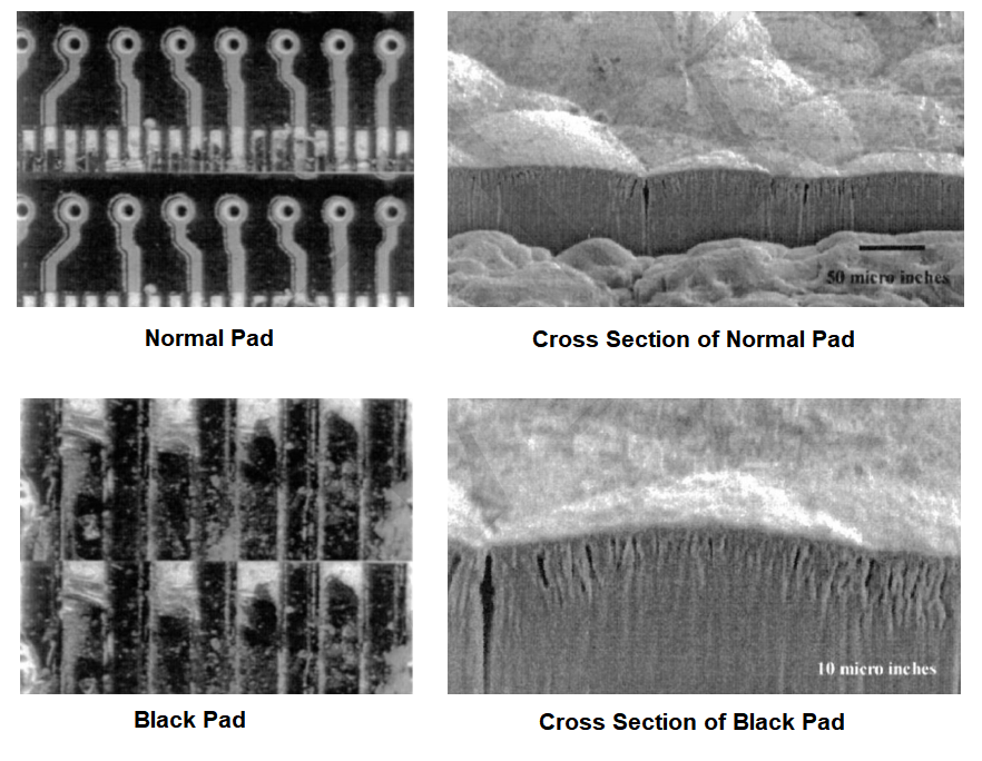
2.2 The addition of phosphorus to the nickel layer can improve the corrosion resistance of the pads and the solder joint reliability
A large number of data and experiments prove that adding phosphorus to the nickel pad will promote the corrosion resistance of the pads and the reliability of the solder joints. The figure below shows the corrosion degree of nickel pads with different phosphorus contents in the SO2 atmosphere[2].
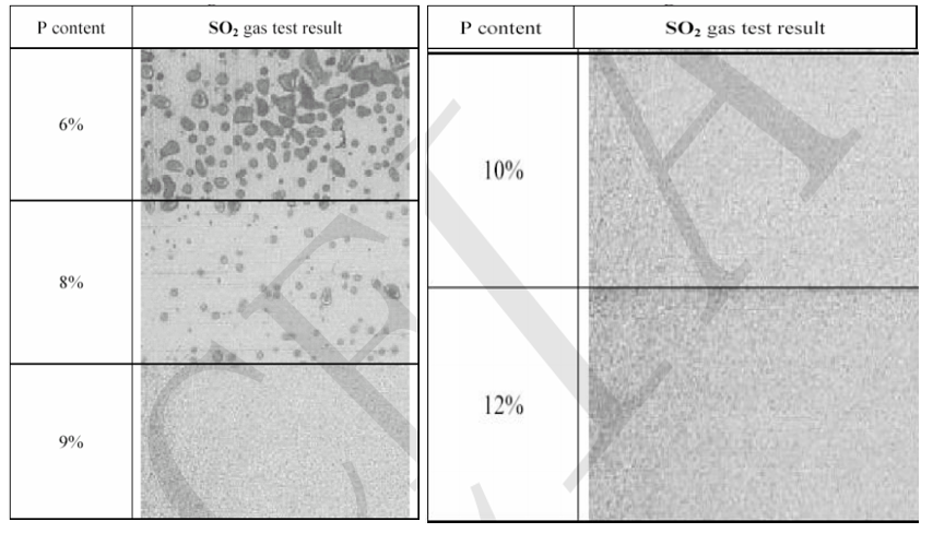
It can be concluded that the corrosion resistance effect of the pads is the best when the nickel layer has a phosphorus content of 9% or higher.
3. The Issues of Immersion Silver
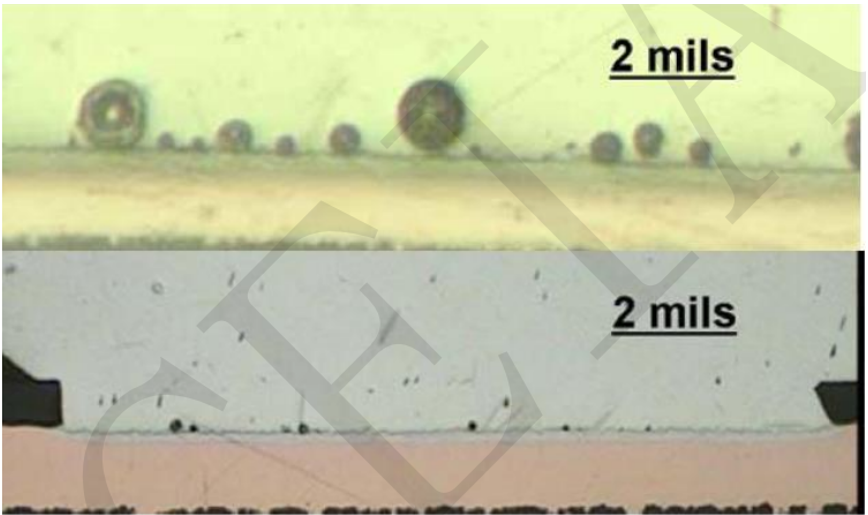
3.1 There are many voids in the cross section of the IMC (0.25mil)
As shown in the figure below, improper soldering produces a number of voids, resulting in the degradation of IMC layer reliability[3],
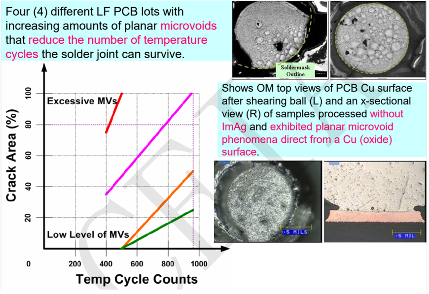
The figure below shows that the corrosion of copper pads is the cause of voids[4].
4. Conclusion
The most basic purpose of surface finishes is to ensure excellent pad solderability and electrical properties and enhance the reliability of the solder joints. Most of the pad material for welding is copper. Since copper tends to exist in the form of oxides in nature, it is unlikely to remain pure copper for a long time. Hence, other treatments are required for copper. During the subsequent assembly, a strong flux can remove most copper oxides. However, a strong flux is rarely used because it is hard to clean. Immersion tin, immersion silver, ENIG, and other surface finishes can effectively ensure extraordinary solderability, electrical properties, and solder joint reliability, which are widely used in semiconductor packaging.
Fitech has been focusing on microelectronics and semiconductor packaging solder for more than 20 years. Fitech is a world-leading packaging material and solution provider for microelectronics and semiconductors. It is a national high-tech enterprise deeply engaged in microelectronics and semiconductor packaging materials. It is the only electronic-grade packaging material manufacturer in the world that can manufacture T2-T10 ultra-fine solder powder. Fitech's solder paste, epoxy solder paste, and alloy solder powder are widely used in microelectronics and semiconductor packaging. The global SMT electronic chemical manufacturers, micro photoelectric manufacturers, and semiconductor packaging testers have recognized the products. However, the problems with microelectronics and semiconductor packaging materials are extensive. We only describe the common problems here. The issues involved may be different because of different technological processes. Welcome to communicate and discuss the specific question with our professionals. We hope to keep pace with the times with our partners and explore new problems, technologies, and complex processes together. Fitech strives to provide partners with professional and thoughtful microelectronics and semiconductor packaging and soldering materials services.
Reference
[1]Zequn Mei, Samuel K. Liem, and Allan Shih, “A Failure Analysis and Rework Method of Electronic Assembly on Electroless Ni / Immersion Au SurfaceFinish”, SMTA, Chicago, IL, 1999.
[2]Masahiro Nozu, Akira Kuzuhara, Atsuko Hayashi, Hiroshi Otake, Shigeo Hashimoto, and Donald Gudeczauskas (C.Uyemura & Co.,Ltd.), “High Phosphorous Electroless Nickel Process for Mobile Phone PWBs”, Apex, S10-1-1, Anaheim, CA, Feb, 2004
[3]Muffadal Mukadam, Norman Armendariz*, Raiyo Aspandiar, Mike Witkowski, Victor Alvarez, Andrew Tong, Betty Phillips, and Gary Long (Intel Corporation), " PLANAR MICROVOIDING IN LEAD-FREE SECOND-LEVEL INTERCONNECT SOLDER JOINTS", SMTAI, September, 2006, Chicago, IL
[4]Muffadal Mukadam, Norman Armendariz*, Raiyo Aspandiar, Mike Witkowski, Victor Alvarez, Andrew Tong, Betty Phillips, and Gary
Long (Intel Corporation), " PLANAR MICROVOIDING IN LEAD-FREE SECOND-LEVEL INTERCONNECT SOLDER JOINTS",
SMTAI, September, 2006, Chicago, IL




 Back to list


