The Failure Modes of Solder Joints (4)
The Failure Modes of Solder Joints (4)
After soldering with lead-free solder paste, intermetallic compound (IMC) growth occurs at the interface of solder pastes and pads. A small amount of IMCs plays a role in solder joint enhancement. However, during the use of components, high temperatures will accelerate the growth of IMCs. Overgrown IMC can form voids at the interface of solder joints and pads, reducing solder joint reliability. This article briefly discusses the effects of IMC growth at the interface of solder joints and copper pads.
The electronic packaging industry usually adopts the ENIG or OSP for surface finishes of the PCBs. The interfacial IMC growth is an important factor affecting the drop performance of solder joints. The interfacial IMC growth is caused by the atomic interdiffusion of solder pastes and pads under thermal stress. Xu et al. (2008) conducted thermal aging tests of solder joints made of SAC305 solder paste (500, 1000, and 1500 cycles, -40℃-125℃). Numerous Kirkendall voids were found at the interface, and the solder joints exhibited interface fractures in the drop test. The pads with ENIG surface finish exhibited vertical voids in the Ni(P) layer at the solder joints (Xu et al., 2008).
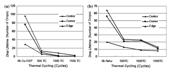
Figure 1 shows the drop test results of the OSP and ENIG treated PCBs. It can be concluded that as the number of thermal cycles increases, the number of drops that the solder joints made of SAC solder paste can withstand decreases rapidly. In addition, the drop resistance of OSP declined significantly. The number of drops reduce almost to less than ten after 500 cycles. The main failure mode is IMC brittle fracture.

Figure 1: Drop test results of solder joints after thermal cycling. (a) is an OSP-treated PCB, (b) is an ENIG-treated PCB ( Xu et al., 2008).
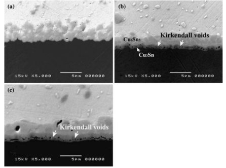
The diffusion rate difference between atoms is the cause of the formation of voids, which is reflected in the presence of vacancies on the side of the metal that diffuses faster. For the OSP-treated PCBs, due to the faster diffusion of Cu atoms and the failure of Sn atoms to fill the vacancies after Cu migration, the vacancies accumulate to form Kirkendall voids. As shown in Figures 2(b) and 2(c), a massive number of voids were found in the Cu3Sn layer, which increases with thermal cycles. The continuity of voids at the interface accelerates the solder joint lift -off.

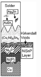
Figure 2: Kirkendall voids grow at the interface of OSP-treated PCB solder joints, a: as-reflowed, b: 500 cycles, c: 1000 cycles ( Xu et al., 2008). Figure 3: The schematic diagram of void formation at the interface of ENIG-treated PCB (Kim et al., 2011).
The NiSnP layer in an ENIG-treated pad showed void formation after thermal cycling. The reason is that the flux of Sn to Ni3P is greater than the flux of Sn from (Cu, Ni)6Sn5 to NiSnP. Diffusion differences lead to the appearance of voids in the NiSnP layer.
Shenzhen Fitech is a manufacturer specializing in the production and sales of packaging solder pastes. Fitech provides high-quality lead-free solder pastes for semiconductor packaging, such as tin-silver-copper solder pastes, tin-bismuth solder pastes, tin-antimony solder pastes, etc.
Reference
Kim, D., Chang, Jh., & Park, J. (2011), “Formation and behavior of Kirkendall voids within intermetallic layers of solder joints”. J Mater Sci: Mater Electron 22. pp.703–716.
Xu, L., Pang, J., & Che, F.X. (2008), “Impact of Thermal Cycling on Sn-Ag-Cu Solder Joints and Board-Level Drop Reliability”. Journal of Electronic Materials. 37. pp.880-886.


 Back to list


