Through-Hole Devices: Influences of Pad and Plated-Hole Dimensions

Through-Hole Devices: Influences of Pad and Plated Hole Dimensions
IC chips usually need to be packaged in ceramic or plastic to protect the chips. The electrical path between the IC chip and the outside needs to be achieved by the leads. The leads need to interconnect with the chip. The lead connection can be realized by either through-hole or surface mount technology. In the application scenarios of high voltage and high power, using through-hole devices is still a preferred solution. For through-hole devices, wave soldering is commonly used, which is achieved by immersing the leads into the molten solder. A series of factors can affect the reliability of solder joints, such as pad area, through-hole size, PCB surface finish, etc. This article briefly introduces the influences of PCB pads and through-hole parameters on the lead-free soldering reliability of through-hole devices.
Sobolewski et al. tested the wave soldering reliability of through-hole devices. (resistors and IC components). The solder used for wave soldering was SAC305 alloy, and the soldering temperature was controlled at 260 ℃. The temperature range and number of thermal cycles were -20-80 ℃ and 550, respectively. In addition, the surface of the PCB was treated by hot air solder leveling, and the pad surface was coated with a lead-free tin-copper-nickel protective layer (SnCu0.7Ni0.05) to prevent copper oxidation.

Figure 1. Layout of the testing devices on the PCB (blue frame), J: resistor (light blue); K: DIP integrated circuit (black).
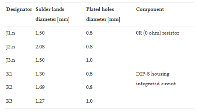
Table 1. Dimensions of plated-holes and pads.
Test result
Soblewski et al. found that the leads of all resistors in the plated holes were completely covered with lead-free SAC305 solder. After SEM observation, it was found that there are almost no voids in the solder joints of resistor J1, which means that the strength of the solder joints remained reliable. A dense IMC layer (Cu, Ni) 6Sn5 was formed between the copper surface and the solder, and the IMC thickness was about 2.5-3.5μm. The reliability of IC K1-K3 after wave soldering was also acceptable, and the (Cu, Ni) 6Sn5 layer was formed on the copper surface.
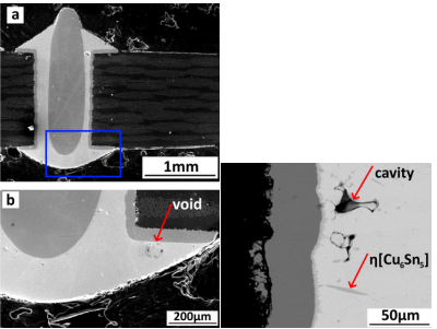
Figure 2. The SEM images of solder joints of resistors J1 (a, b) and J3 (right).
The (Cu, Ni)6Sn5 phase enriched with nickel grows in the form of dispersed precipitates in the solder matrix. It is important that the nickel composition in the (Cu, Ni) 6Sn5 phase can affect the phase morphology and accelerate the growth of the (Cu, Ni) 6Sn5. In addition, the existence of nickel inhibited the growth of deteriorated IMC Cu3Sn. Sobolewski et al. also revealed that with the increase of through-hole diameter and pad size, the possibility of solder joint defects increased. The through-hole size of resistor J3 was the largest, and the number of corresponding cavities was more than J1 (Figure. 2). Similarly, K2 and K3 had larger through-hole and pad sizes. Therefore, more voids or cracks occurred in the solder joints after wave soldering.
Thermal cycling test
After 550 thermal cycles, the solder joints of both resistors and ICs faced a greater risk of failure. The number of voids increased as the thermal cycle proceeded. When the voids accumulated to a certain extent, the aggregation of voids formed microcracks, which caused the solder joint to fracture easily under external force. No obvious microcracks were found in J1-J3, but a higher number of voids were detected in J2 and J3. The solder joint of K3 cracked after thermal cycling, which represents that the mechanical strength of the solder joint decreased. It is clear that the size of the pad and through-hole has an obvious impact on the reliability of solder joints.
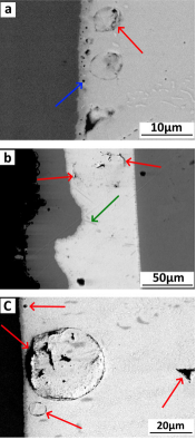
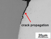
Figure 3. The microstructure of solder joints after thermal cycling, (a) J1; (b ) J2; (c) J3; (right) K3.
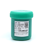
With the surface-mount technology trending to replace through-hole technology, Shenzhen Fitech has produced ultrafine lead-free solder paste products for surface-mount devices, which are suitable for ultra-fine-pitch and high-density soldering. The solder joints formed after reflow soldering have high reliability and outstanding electrothermal performance.
Reference
Sobolewski, M., Wojewoda-Budka, J., Huber, Z., Zieba, P. & Wierzbicka-Miernik, A. (2021). “Solder joints reliability of through hole assemblies with various land and hole design”. Microelectronics Reliability, vol.125.




 Back to list


