Solder Paste for IGBTs: Power Cycle Test and Control Strategy for IGBTs
Solder Paste for IGBTs: Power Cycle Test and Control Strategy for IGBTs
Solder Paste and Ultra-Fine Solder Manufacturer-Shenzhen Fitech is a comprehensive solder paste supplier integrating production, sales, research, and service of solder paste, epoxy solder paste, and solder powder. Fitech is the leading unit for the formulation of solder powder standards of the Ministry of Industry and Information Technology. Fitech's products include ultra-fine lead-free printing solder paste, ultra-fine lead-free dispensing solder paste, ultra-fine lead-free jetting solder paste, ultra-fine lead-free pin transfer solder paste, no-clean solder paste, water-soluble solder paste, high-temperature solder paste, medium-temperature solder paste, low-temperature solder paste, etc. Fitech can manufacture electronic-grade packaging solder powders with particle sizes from T2-T10.

Introduction
The power cycle test is a reliability test method for IGBTs, which is listed as a must-test item in vehicle-level test standards for AEC-Q101 and AQG-324. Compared with the temperature cycle test, the power cycles generate heat through the chips working inside the devices so that the devices reach a predetermined temperature. However, the temperature cycles are to force the device under test to reach the test temperature through the external environment.
In short, one is exercise fever, and the other is high-temperature heatstroke.
Fitech
Power Cycle Test
Power Cycle Test
Since the heating part of the device under test in the power cycle test is concentrated in the device working area, its packaging aging mode is similar to that of the device under normal operation. Hence, the power cycle test is the reliability testing that has received extensive attention because it is highly close to the actual application scenario.
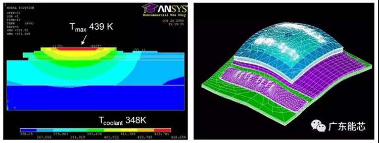
During the power cycle test, the temperature distribution and stress change inside the device.
Power Cycle Test Bench
The power cycle test bench is a device used for power cycle tests of IGBT devices, and its design principle is not complicated. In the test bench, the load current is supplied to the device through the current source. The current probe monitors the current data of the device in real-time. The controller manipulates the current source to interrupt the load current at a predetermined time. The main cost of the whole equipment is attributed to the current source and the controller. The design difficulty of the equipment lies in the program control and data acquisition hardware.
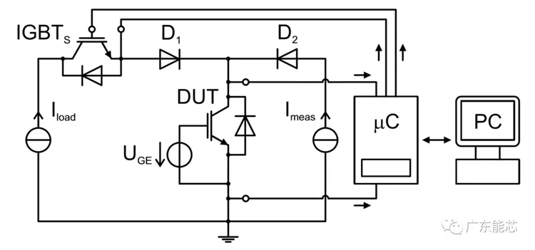
Schematic diagram of power cycle test equipment
Detection Time Points and Measured Parameters
During power cycling testing, the data directly detected are device voltage drop, load current, and device bottom temperature. By selecting the time point of data sampling, the voltage of the device and the temperature change of the bottom of the device at the highest temperature and the lowest temperature are collected. After that, the temperature change of the device chip and the thermal resistance change inside the device can be obtained by calculation.

Detection time points and the parameters
Since most devices are in a packaged state during the test, their internal temperature cannot be detected by direct means. Therefore, in the power cycle test, the temperature of the internal chip of the device is obtained by indirect calculation using the K coefficient. The K coefficient represents the temperature-sensitive electrical parameter of the device chip. The principle of its selection is simplicity, reliability, and high sensitivity. The temperature of a silicon-based IGBT chip is generally calculated using Vce (collector-emitter voltage). At the same time, Vce can reflect the aging of the internal current path of the IGBTs. A 5% increase in Vce is recognized as the standard for device damage.
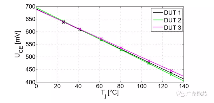
K Coefficient of IGBT Device (VCE-TJ Fitting line)
The thermal resistance of the device should be monitored in real-time during power cycling because it reflects changes in the device's ability to dissipate heat. The thermal resistance is simply calculated by the following equation, and a 20% increase in Rth is considered the criterion for device failure.

Taking the data collected in the following power cycle test as an example, Vce has a phase jump around 427.4k cycles, and the maximum temperature (Tj, high) of the device chip rises significantly, indicating that the bonding wires on the surface of the device chip are broken or fall off. However, there is no significant change in Rth, indicating that the aging of the heat dissipation layer inside the device is negligible.
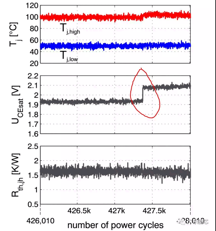 Data in the IGBT cycle test
The power cycle test data in the above figure has a defect of noisy test data, which cannot accurately reflect the real situation inside the device. The reasons for this defect are that the electrical connection of the device under test is not standardized, the accuracy of the power cycle test equipment is limited, the selection of the test data monitoring time point is improper, and so on.

SAC Solder Paste SACS Solder Paste SnBiAg Solder Paste SnBiAgSb Solder Paste SnBiAgX Solder Paste SnBi Solder Paste BiX Solder Paste AuSn Solder Paste SnSb Solder Paste SnPb Solder Paste Anisotropic Conductive Paste Ultra-Fine-Pitch Flux

IFitech
Power Cycling Test-Control Strategy
Power Cycling Test-Control Strategy
In the Power cycle test, the testing device reaches the preset temperature through the heat generated by its power loss. The basic relationship between the device junction temperature and other parameters is summarized by the following formula.

It can be seen from the formula that the device junction temperature (Tj) required for the test can be adjusted by changing the power loss (I*V), thermal resistance (Rth), and cooling plate temperature of the device (Tc is the case temperature that approximately equals to the cooling temperature). Additionally, the on-time (ton) of the device will affect the junction temperature of the device.
In the previous introduction, the standard power cycle test is realized by the test circuit shown in the figure below. The device is tested with a fixed on-time, cool-down time, and load current. As the keys and wires and the solder layer gradually age during the test process, the power loss of the device increases, and the heat dissipation of the device deteriorates. The interaction of the defect factors causes the junction temperature of the device to rise and further accelerates the damage to the device package, eventually leading to device failure.

Schematic diagram of power cycling test equipment
Power Cycling Test-Test Summary
However, the control strategy of the power cycle test is more than one. The case temperature Tc, power loss Pv, and junction temperature Tj can all be kept constant during the test by adjusting other parameters to measure the power cycle life of the device in different operating environments. U. Scheuermann, G. Zeng, and others have conducted in-depth research on the impact of control strategies.
In the study of U. Scheuermann, the case temperature difference (dTc), power loss (Pv), and junction temperature difference (dTj) were fixed through different parameter tuning during the test process. The initial junction temperature difference (dTj) of the device was 125 Kelvin. The final test results show that the standard power cycle test was more stringent than the test using other test control strategies, and the test life of the device was the shortest. However, the type of test control strategy did not affect the failure mechanism of the devices, which all failed due to the bond and wire detachment. The situation of the solder layer on the bottom of the chip was not reflected in the research of U. Scheuermann.
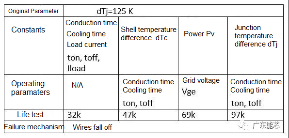
U. Scheuermann, Summary of power cycle tests under different control strategies
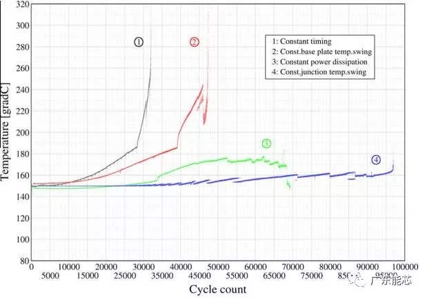
U. Scheuermann, Results of power cycling testing under different control strategies
The bonds and wires in the figure below are blown due to the uneven distribution of temperature and current. This phenomenon mainly occurs after some keys and wires fall off, and the rest cannot load the conduction current.
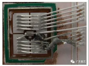
U. Scheuermann, bonding failures caused by power cycle testing
In G. Zeng's study, the power loss (Pv) and the junction temperature difference (dTj) were fixed during the test, and the selected control parameters were more refined than those in U. Scheuermann's study. However, compared with 125 K, the initial experimental condition of the junction temperature difference dTj=87 K has a larger gap, resulting in different failure mechanisms (solder layer aging failure). Therefore, it is impossible to directly compare the two experiments. However, the similarity is that fixed turn-on and cooling time were still the most stringent test control strategies in G. Zeng's research.
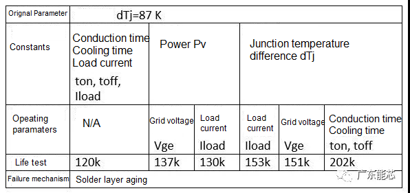
G. Zeng, Power cycling test summary under different control strategies
The figure below is the monitoring parameter curve obtained in the power cycle test. It can be clearly seen that the junction temperature difference (dTj) and the thermal resistance value (Rth) changed synchronously during the test process. This type of test parameter curve appears mostly in tests with low junction temperature differences.
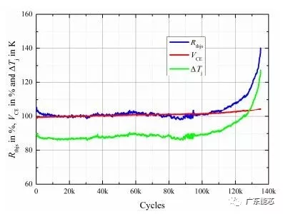
G. Zeng, Parameter monitoring in standard power cycle tests
Solder layer aging at the bottom of the chip can be visually compared by ultrasonic scanning microscopy.
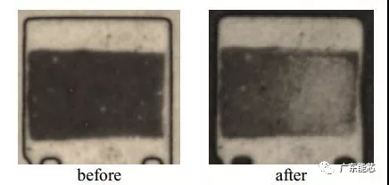
G. Zeng, Failure of solder layer at the bottom of chip caused by power cycling test
Power Cycling Test-Standard Control Strategy
From the existing research, it is clear that the standard power cycle test control strategy is the method of fixing the conduction and cooling time and the load current, which can obtain the power cycle test life of the device most quickly. This control strategy is adopted by the majority of manufacturers due to its simple test operation, simple equipment structure, high efficiency, and close to the actual application scene. Other types of test control strategies exist only for special test needs.
In IEC, AQG324, and other test standards, the control strategy of fixed conduction and cooling time is listed as the standard test operation specification. The test standard method cannot work by changing the test control strategy to prolong the test life of the device.

Source: Powersemiled





 Back to list


