Preparation and Common Problems of ENIG PCB-Shenzhen Fitech

Preparation and Common Problems of ENIG PCB-Shenzhen Fitech
There are many methods of PCB surface finishes, including OSP, silver plating and gold plating. There is a widely used surface finish technology called eletctoless nickel/immersion gold (ENIG). Compared with the gold-plated PCB, the gold layer of the ENIG PCB is thinner, but the compactness is slightly poor. The thickness of the gold and nickle layers of the ENIG PCB are generally controlled at 0.05-0.1μm and 3-5μm, respectively. The gold layer not only conduct electricity and slow down corrosion but also protect the nickel layer from oxidation, maintaining excellent soldering ability.

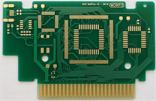
Figure 1. An image of ENIG PCB.
Preparation of ENIG PCB
The copper surface of the PCB needs to be cleaned before the ENIG process. The reducing agent (such as sodium hypophosphite) in the nickel tank reduces the bivalent nickel to nickel atoms that deposit on the copper surface under the temperature impact. During the reaction, the univalent phosphorus of sodium hypophosphite will be oxidized to trivalent phosphorus or pentavalent phosphorus. Phosphorus atoms will appear in the nickel layer along with the growth of the nickel layer. The content of the phosphorus atom in the nickel layer is 7-8%, which is called medium phosphorus content. For high phosphorus content, the phosphorus proportion increases to 9-11%. Whether the content of phosphorus is medium or high, the nickel layer is formed by nickel nodules. Big nickel nodules will lead to unevenness of the coating surface and reduce the subsequent immersion gold quality.
After electroless nickel, PCB is ready for gold immersion. The immersion gold is a chemical displacement reaction. The nickel plating layer of the PCB is oxidized in the gold immersion tank to release two electrons. The electrons obtained from free gold are reduced and deposited on the surface of the nickel layer. As the redox reaction proceeds, the gold layer gradually thickens until the reaction between the bath solution and the nickel layer is blocked.
“Black pad” phenomenon
Sometimes, after removing the failed solder joint, you will see a black surface, which is most likely a black pad. There are two main reasons for the appearance of the black pad.
(1) Rough copper surface leads to large height drop of nickel surface, which leads to the failure of gold deposition to each dead corner during gold deposition, leading to the oxidation of the nickel layer and black disc.
(2) The speed of gold deposition has not been effectively controlled. The thickness of the gold layer is uneven due to the inconsistent speed of gold deposition. The thinner the gold layer is, the more likely it is to be permeated by the bath solution. The bath solution penetrating into the gold layer will oxidize the nickel layer. Nickel oxide leaves the nickel layer and accumulates on the copper surface. However, the adhesion of nickel oxide is insufficient and it is difficult to react with copper metallurgically, leading to the solder joint strip-off problem.
Undissolved gold layer
The undissolved gold layer of the pad represents the failure of the gold layer to dissolve into the molten solder paste after reflow. In this case, the pad surface remains golden after reflow. The insolubility of the gold layer on the pad of the ENIG PCB can be considered as the contamination of the gold layer by the gold bath solution or the incomplete cleaning in the subsequent process and the oxidation of the nickel layer. In addition, under normal circumstances, the gold deposit should not contain impurities such as nickel, copper, etc. Once the gold layer contains some inappropriate impurity elements, it is easy to cause poor solderability.
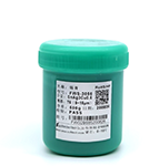
Shenzhen Fitech can provide solder paste products for ENIG PCB soldering. Fitech’s solder paste has good wettability and viscosity and can be printed on the pad through the stencil smoothly. During soldering, the solder paste can react with the pad quickly to form an IMC layer. Welcome to contact us.


 Back to list


