Copper Pillar Bump Solder Paste _Copper Pillar Bump Reliability

Copper Pillar Bump Solder Paste _Copper Pillar Bump Reliability
The pitch and size of solder joints continue to shrink as the need for small chip sizes and higher I/O densities. Copper pillar bumps in flip-chip enable finer pitches and greater electromigration resistance but introduce higher stress. Electroplated solder bump (area array) devices are limited to a minimum pitch of 140µm–180µm. Therefore, when the solder joint pitch is less than 140μm, copper pillar bumps are usually used.
Solder joint reliability is a topic of concern. Li et al. obtained Cu/Sn-Ag/Cu and Cu/IMC/Cu bump structures through a hot bar bonding process and performed thermal cycling tests to compare their failure modes. The end of the connection between the copper pillar and the substrate has a SnAg3.5 solder paste with a thickness of about 20 μm.

Figure 1. Schematic diagram of hot pressing soldering.
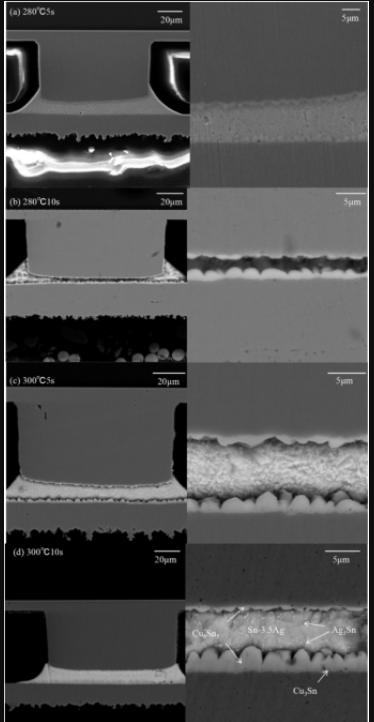
It can be seen from Figure 2 that with the increase in temperature or time, the thickness of the IMCs on the substrate side increases significantly. The reaction that occurs during the hot bar bonding process is mainly solid-liquid diffusion. The Cu atoms in the Cu pillar bumps dissolve into the solder Sn. When the dissolved Cu atoms in the solder Sn near the interface are saturated, scalloped Cu6Sn5 and a small amount of Ag3Sn are generated at the interface. If the bonding temperature is higher than 300°C and the holding time is longer than 10s, a thin Cu3Sn layer will form under the Cu6Sn5 layer.

Figure 2. IMC growth under different soldering conditions.
Copper Pillar/Sn-3.5Ag/Pad Bump Failure Mode
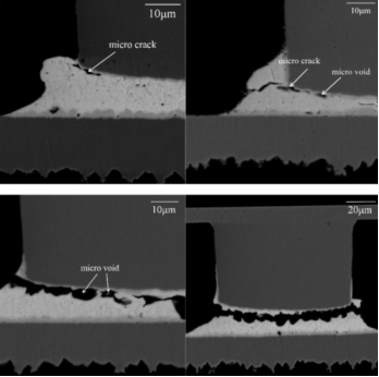
In the beginning, it can be observed that cracks occur at the corners of the copper pillar solder joints, and then the voids begin to grow inside the solder joints. Voids build up under stress and cause the solder joints to break. The location of the crack mainly appears at the interface of the IMC and the solder on the side of the copper pillar or inside the solder near the interface.

Figure 3. Solder joint fracture evolution.
Sn-Ag solder joints undergo creep and stress relaxation under cyclic stress. Dislocation loops form near particles such as Cu6Sn5 and Ag3Sn in the solder and then gradually nucleate and continue to grow into elliptical voids. In solder paste solder at the edge of copper pillars, fatigue cracks are mainly caused by concentrated stress. The crack then grows inward and combines with the void, eventually penetrating the entire solder joint along the interface of the copper pillar.
Copper pillar/IMC/Pad
The solder will gradually convert to IMC during thermal cycling. Cracks mainly occur at the interface of Cu6Sn5 and Cu3Sn on the substrate side. The main failure mode is characterized by interfacial delamination at the interface of Cu6Sn5 and Cu3Sn on the substrate side. The Cu6Sn5 grains on both sides fracture and finally the Sn solder on both sides penetrates the entire solder joint. The failure mode of solder joints is a brittle fracture.
Shenzhen Fitech can produce high-reliability ultrafine solder adhesive products (epoxy resin-based solder paste). After soldering, the epoxy resin is thermally cured and wrapped around the solder joints to protect the solder joints. Welcome to contact us for more information.
Reference
Li, J.H., Zhang, Y.X., Zhang, H.L., Chen, Z., Zhou, C., Liu, X.H. & Zhu, W.H. (2020). The thermal cycling reliability of copper pillar solder bump in flip chip via thermal compression bonding. Microelectronics Reliability, vol.104.


 Back to list


